
Semiconductor memory device

A storage device and semiconductor technology, applied in the direction of information storage, static memory, digital memory information, etc., can solve the problems of high power consumption, slow action speed, etc., to suppress the influence of crosstalk, expand the interval between wiring, reduce Effect of inter-wiring capacitance

Inactive Publication Date: 2007-12-19
SANYO ELECTRIC CO LTD
View PDF1 Cites 0 Cited by
  • Summary
  • Abstract
  • Description
  • Claims
  • Application Information

AI Technical Summary

Problems solved by technology

At this time, when all the memories are precharged, the power consumption is large, and the operation speed becomes slow.

Method used


Image

  • Semiconductor memory device
  • Semiconductor memory device
  • Semiconductor memory device

Examples


Embodiment Construction

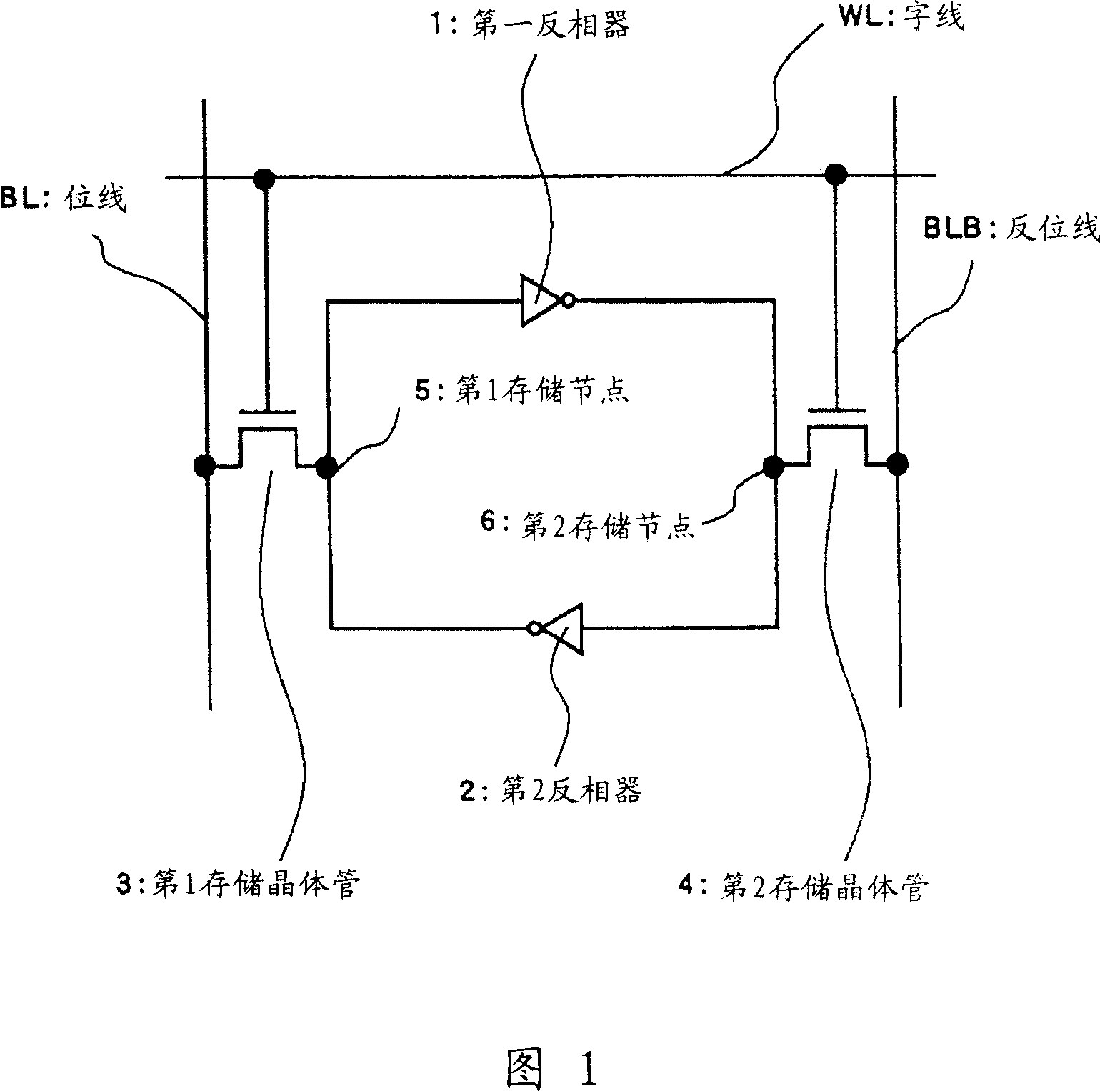
[0026] Hereinafter, the semiconductor memory device of the present invention will be described in detail with reference to the drawings.

[0027] First, the memory cell of the semiconductor memory device of the present invention will be described.

[0028] FIG. 1 is a diagram showing an SRAM used as a memory cell.

[0029] The first inverter 1 and the second inverter 2 constitute a latch circuit in which inputs and outputs are cross-connected. Furthermore, the gates of the first access transistor 3 and the second access transistor 4 are commonly connected to the word line WL. Next, the first access transistor 3 and the second access transistor 4 are respectively connected to the first storage node 5 and the second storage node 6 , the bit line BL and the reverse bit line BLB.

[0030] The above SRAM operates as follows. That is, first, the bit line BL and the reverse bit line BLB are applied with an H potential to be in a precharged state. Next, in the precharge state, H p...


PUM


Abstract

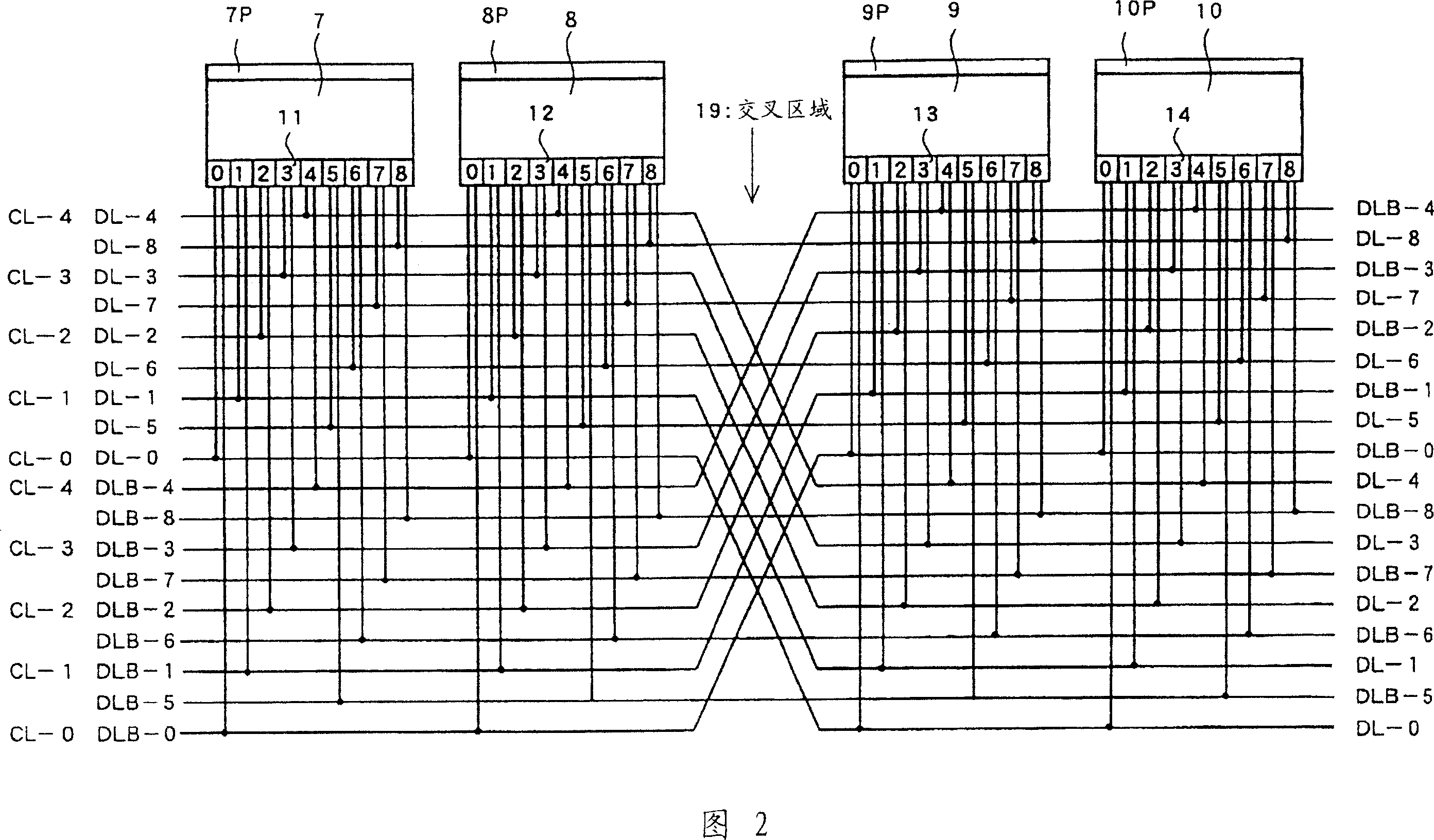
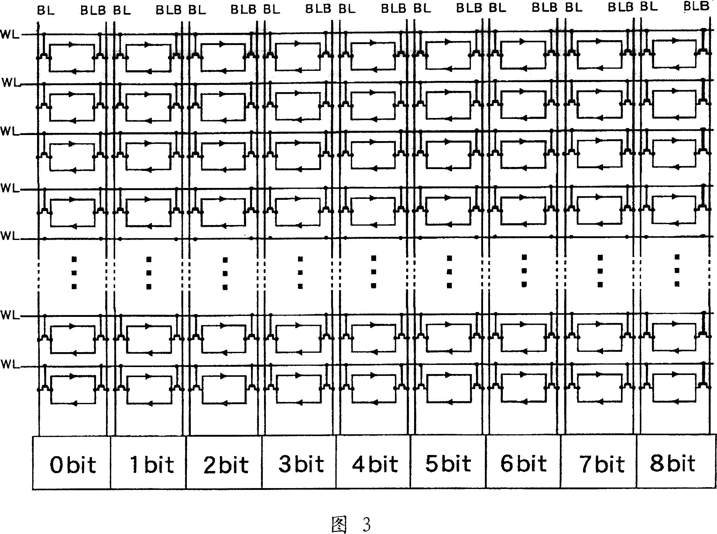
According to some preferred embodiments of the present invention, a semiconductor memory device includes an array of memory cells and plural pairs of complementary bit lines, each pair of the complementary bit lines being connected to the memory cells arranged in the same column. The array is divided into plural memory blocks each including plural memory cells arranged in the same column. The corresponding complementary bit lines of the plural memory blocks are connected to corresponding common complementary data lines, respectively. Some pairs of the complementary data lines are crossed at least one time so that the complementary data lines of each pair of the some pairs of the complementary data lines are reversed in position and that the crossed data line and a non-cross data line are arranged alternately whereby crosstalk to be generated between adjacent data lines are reduced.

Description

technical field [0001] The present invention relates to a semiconductor storage device, and more particularly to a semiconductor storage device with SRAM (static random access memory). Background technique [0002] When power is applied, SRAM is a RAM that can be written or read at any time without a refresh operation. [0003] FIG. 1 shows an SRAM used as a memory cell. [0004] A first inverter (inverter) 1 and a second inverter 2 constitute a latch circuit in which inputs and outputs are cross-connected. In addition, the gates of the first access transistor 3 and the second access transistor 4 are commonly connected to the word line WL. Furthermore, the first access transistor 3 and the second access transistor 4 are respectively connected to the first storage node 5 and the second storage node 6 , the bit line BL and the reverse bit line BLB. [0005] Such an SRAM is used as a memory of a microcomputer. For example, a microcomputer such as an LCD driver for driving a ...

Claims


Application Information

Patent Timeline
Patent Type & Authority Applications(China)
IPC IPC(8): G11C11/41G11C11/413G09G3/36
CPCG11C7/18G11C7/02G11C11/417G11C5/063
Inventor 三谷和之
Owner SANYO ELECTRIC CO LTD
Learn More