Wiring board, method for manufacturing the same, and semiconductor device
A technology for wiring substrates and semiconductors, which is applied in the fields of semiconductor devices, semiconductor/solid-state device manufacturing, and semiconductor/solid-state device components, etc., can solve problems such as decreased bonding strength of conductor wiring 23 and insulating substrate 22, no bonding, etc.
- Summary
- Abstract
- Description
- Claims
- Application Information
AI Technical Summary
Problems solved by technology
Method used
Image

Examples
no. 1 Embodiment approach
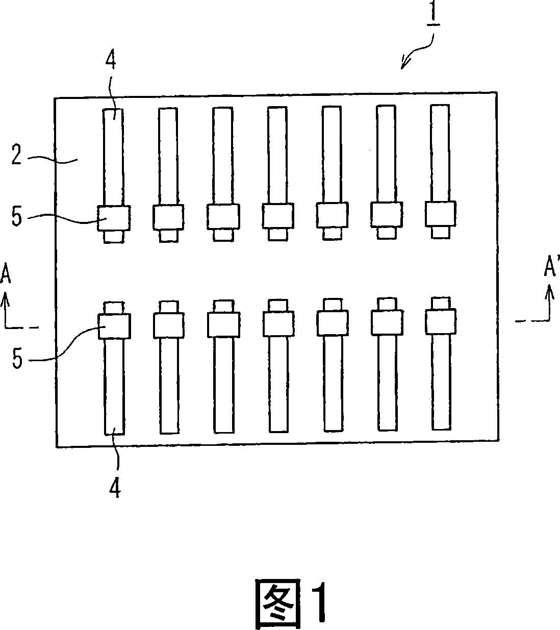
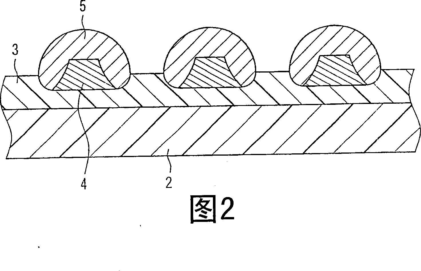
[0039] FIG. 1 is a plan view showing a wiring board 1 according to a first embodiment of the present invention, and FIG. 2 is a cross-sectional view showing A-A' of FIG. 1 .
[0040] In FIGS. 1 and 2 , 2 is an insulating base material, 2 is an adhesive layer formed on the surface of the insulating base material 2 , and 4 is a conductor wiring formed on the adhesive layer 3 . Protruding electrodes 5 are formed across regions on the adhesive layer 3 on both sides of the conductor wiring 4 across the longitudinal direction of the tip portion of the conductor wiring 4 . As shown in FIG. 2 , the back surface of the conductor wiring 4 in the area where the protruding electrode 5 is formed and the back surface and a part of the side surface of the area of the protruding electrode 5 formed on the adhesive layer 3 on both sides of the conductor wiring 4 are bonded together. The surface of the layer 3 is recessed inwardly, and is adhered to the adhesive layer 3 .
[0041] Here, a fle...
no. 2 Embodiment approach
[0047] The wiring board in the second embodiment of the present invention has the structure shown in cross-sectional view in FIG. 2 above.
[0048] In the cross-sectional view of FIG. 2 , the width of the protruding electrodes 5 formed across the lengthwise direction of the conductor wiring 4 and across the regions on the adhesive layer 3 on both sides of the conductor wiring 4 is wider than the width of the back surface of the conductor wiring 4 , In addition, the surface of the area from the back surface of the conductor wiring 4 to the side surface of the protruding electrode 5 via the back surface of the protruding electrode 5 is smoothly formed in a convex shape. Parts of the rear surface and side surfaces of the protruding electrodes 5 are recessed from the surface of the adhesive layer 3 and bonded to the adhesive layer 3 .
[0049] According to the second embodiment, no gap is formed between the side surface of the protruding electrode 5 and the adhesive layer 3, and t...
no. 3 Embodiment approach
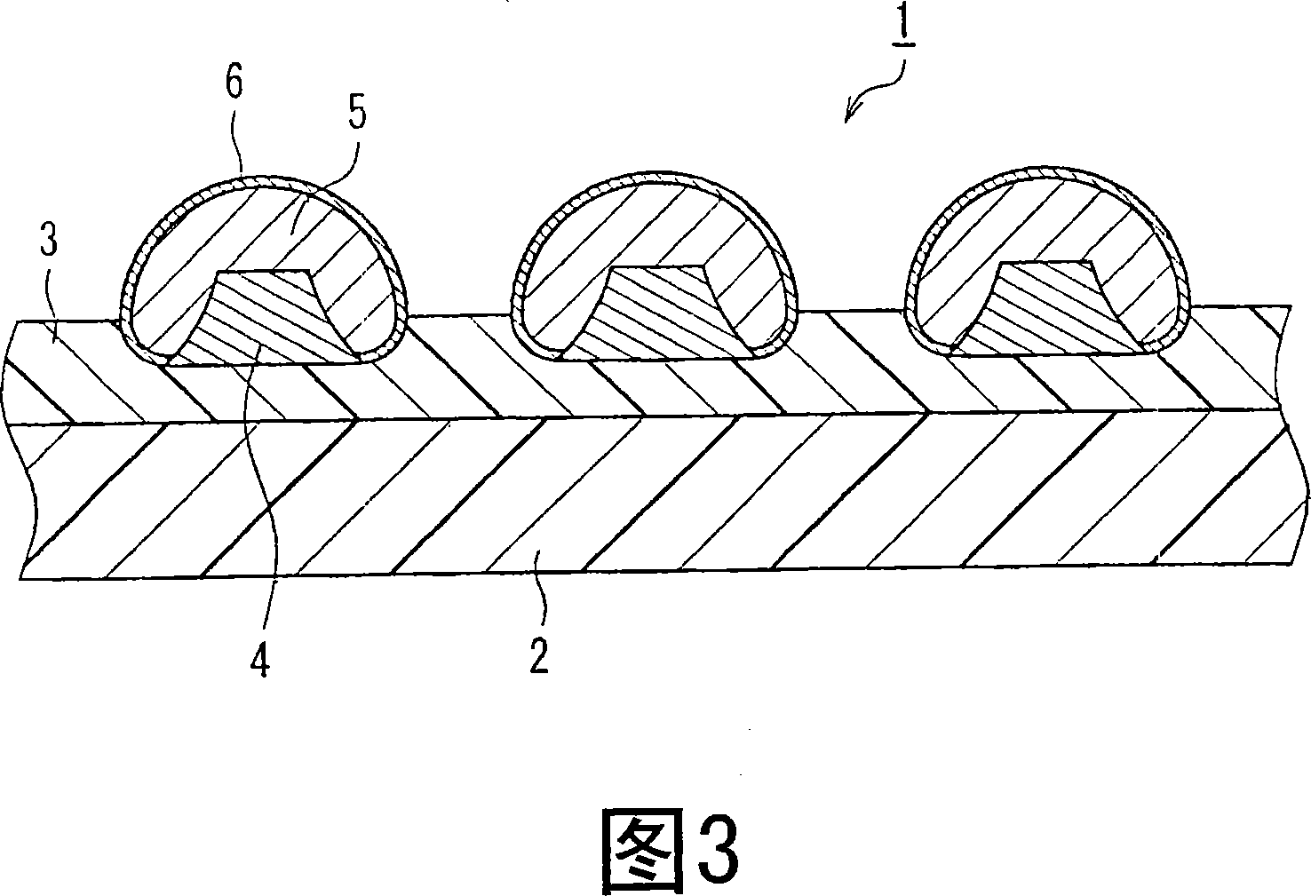
[0051] FIG. 3 is a cross-sectional view showing wiring board 1 in a third embodiment of the present invention. In FIG. 3, the insulating base material 2, the adhesive layer 3, the conductor wiring 4, and the protruding electrodes 5 are the same as those of the first embodiment. Furthermore, a first conductive layer 6 is provided to cover the protruding electrodes 5 , and the back and side surfaces of the protruding electrodes 5 and the adhesive layer 3 are bonded together through the first conductive layer 6 .
[0052] Here, the first conductive layer 6 is formed to have a thickness of about 0.3 μm to 2 μm, for example, by electrolytic Au plating. In addition, Au is formed with a thickness of about 0.5 μm in consideration of the barrier properties and materials of the first conductive layer 6 . In addition, the first conductive layer 6 may be formed of various materials, for example, the bottom layer may be Ni with a thickness of about 1 μm, and the surface layer may be Au wi...
PUM
| Property | Measurement | Unit |
|---|---|---|
| Thickness | aaaaa | aaaaa |
| Thickness | aaaaa | aaaaa |
| Thickness | aaaaa | aaaaa |
Abstract
Description
Claims
Application Information
 - Generate Ideas
- Intellectual Property
- Life Sciences
- Materials
- Tech Scout
- Unparalleled Data Quality
- Higher Quality Content
- 60% Fewer Hallucinations
Browse by: Latest US Patents, China's latest patents, Technical Efficacy Thesaurus, Application Domain, Technology Topic, Popular Technical Reports.
© 2025 PatSnap. All rights reserved.Legal|Privacy policy|Modern Slavery Act Transparency Statement|Sitemap|About US| Contact US: help@patsnap.com