Epitaxial wafer growth method for improving galliumnitride base LED chip antistatic capability
An LED chip, GaN-based technology, applied in circuits, electrical components, semiconductor devices, etc., can solve problems such as failure and failure of LED devices, and achieve the effect of improving crystal quality and anti-ESD yield.
- Summary
- Abstract
- Description
- Claims
- Application Information
AI Technical Summary
Problems solved by technology
Method used
Image
Examples
Embodiment Construction
[0022] Growth by MOCVD method:
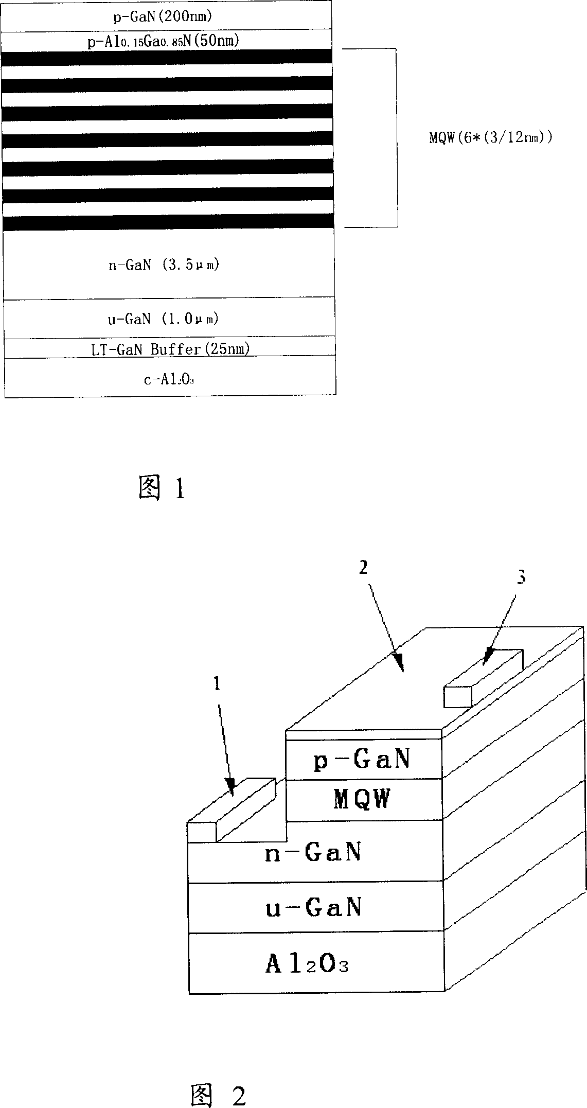
[0023] 1) Load the (0001) no-clean sapphire substrate into the reactor, and 2 Heat to 1100°C and bake for 10 minutes under atmosphere.
[0024] 2) Cool down to 550°C to grow LT-GaN Buffer with a thickness of 25nm, the growth pressure is 300Torr, the TMGa flow rate is 130 micromol / min, NH 3 The flow rate was 150 mmol / min.
[0025]3) A u-GaN layer with a thickness of 1.0 μm was grown at 1050 ° C, the growth pressure was 300 Torr, the flow rate of TMGa was 515 micromol / min, NH 3 The flow rate was 480 mmol / min.
[0026] 4) An n-GaN layer with a thickness of 3.5 μm was grown at 1050° C., the growth pressure was 200 Torr, the flow rate of TMGa was 650 μmol / min, and NH 3 The flow rate is 900 mmol / min, and the amount of Si doped in the n-GaN layer is 55 nmol / min.
[0027] 5) Grow 6 cycles of MQW layer under N2 atmosphere, the growth pressure is 200Torr, NH 3 The flow rate is 1000 mmol / min, InGaN well layer: thickness is 3.0nm, growth temperature ...
PUM
 Abstract
Description
Claims
Application Information
 - R&D Engineer
- R&D Manager
- IP Professional
- Industry Leading Data Capabilities
- Powerful AI technology
- Patent DNA Extraction
Browse by: Latest US Patents, China's latest patents, Technical Efficacy Thesaurus, Application Domain, Technology Topic, Popular Technical Reports.
© 2024 PatSnap. All rights reserved.Legal|Privacy policy|Modern Slavery Act Transparency Statement|Sitemap|About US| Contact US: help@patsnap.com


