
Electronic device and method of communication resource allocation

A technology for electronic equipment and communication resources, which is applied in electrical components, digital transmission systems, transmission systems, etc., and can solve problems such as difficulty in providing latency guarantees and high buffering costs.

Inactive Publication Date: 2007-10-10
NXP BV
View PDF0 Cites 0 Cited by
  • Summary
  • Abstract
  • Description
  • Claims
  • Application Information

AI Technical Summary

Problems solved by technology

Contention can occur at each network node, making it difficult to provide latency guarantees
Using schemes such as rate-based switching or deadline-based packet switching can still provide throughput guarantees (i.e., guaranteed throughput GT), but at the expense of high buffering

Method used


Image

  • Electronic device and method of communication resource allocation
  • Electronic device and method of communication resource allocation
  • Electronic device and method of communication resource allocation

Examples


Embodiment Construction

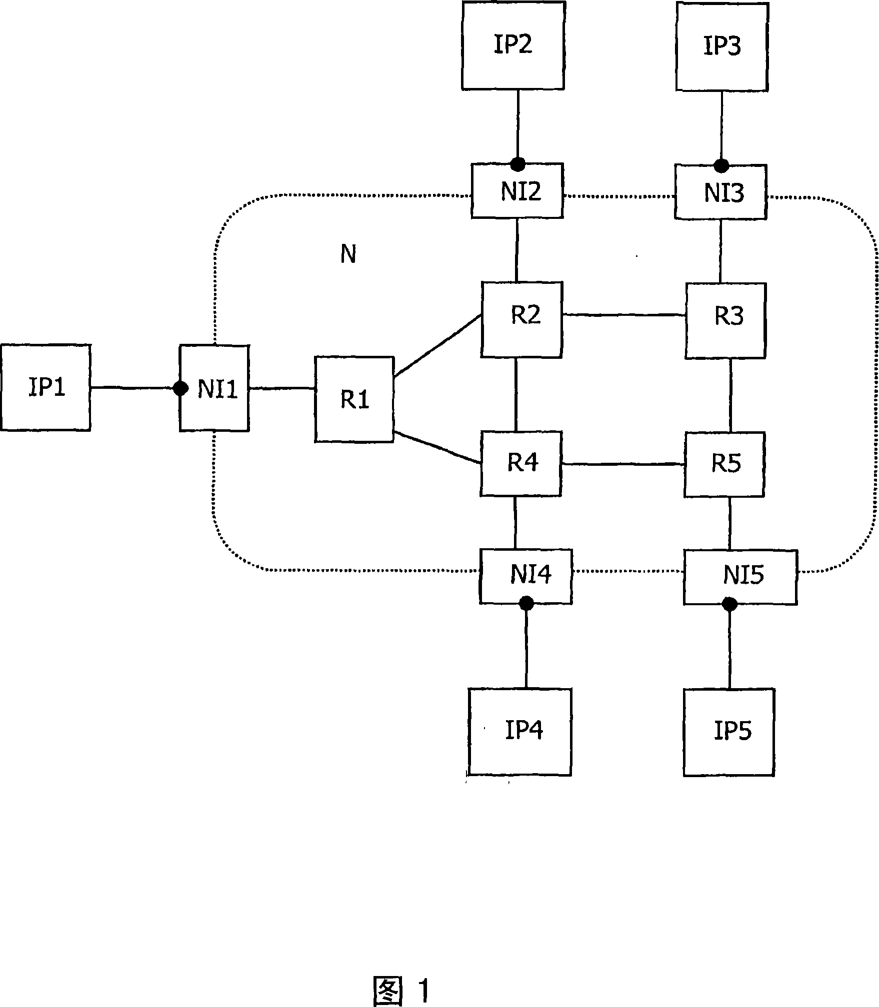
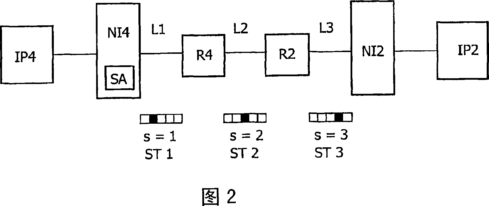
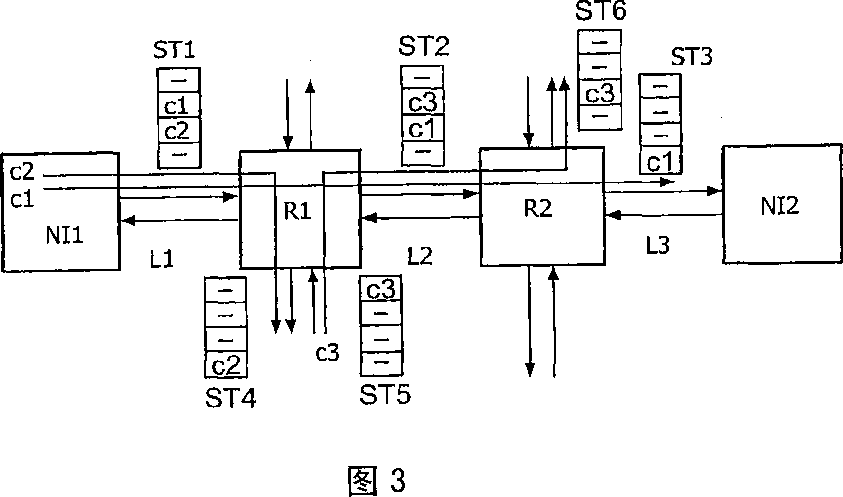
[0034] The following embodiments relate to a system on a chip, ie multiple modules on the same die, multiple dies (eg system in package) or multiple chips, which communicate with each other via some interconnect. This interconnect is embodied as a system on chip NOC. A system on a chip may include wires, buses, time division multiplexes, switches, and / or routers in a network. At the transport layer of the network, communication between modules is performed over connections. A connection is considered to be a set of channels between a first module and at least one second module, each channel having a set of connection characteristics. For a connection between a first module and a single second module, the connection may include two channels, i.e. one channel from the first module to the second module (i.e. the request channel) and a second channel from the second to the first module Two channels (ie, response channels). Thus, a connection or connection path (ie, connection p...


PUM


Abstract

Therefore, an electronic device is provided having a plurality of processing modules (IP1-IP5), an interconnect means (N) for coupling the plurality of processing modules (IP1-IP5) enabling at least one first communication (CII) among the processing modules (IPI-IP5), and at least one first module (D1-D5; NI1-NI7) for communicating with one of the plurality of processing modules (IP1-IP5) through the interconnect means (N) based on at least one second communication (CI). A second communication (CI) is established which is non-intrusive with regards to the first communication (CII).

Description

technical field [0001] The invention relates to an electronic device having a plurality of processing modules and interconnection means for connecting said plurality of processing modules (IP1-IP5), and a method of communication resource allocation within such an electronic device. Background technique [0002] Systems on silicon exhibit a continuous increase in complexity due to the increasing need to implement new features and improve existing functions. This is achieved by increasing the density at which components are integrated on an integrated device. At the same time, the clock speed at which the circuits are operated also tends to increase. Higher clock speeds and increased component density reduce the area that can operate simultaneously within the same clock domain. This creates a need for a modular approach. According to this approach, the processing system includes a plurality of relatively independent and complex modules. In conventional processing systems, ...

Claims


Application Information

Patent Timeline
IPC IPC(8): H04L12/56
CPCH04L45/00H04L45/40H04L47/10H04L49/109
Inventor 卡林·乔尔达什克斯·G·W·戈森斯安德烈·勒杜列斯库
Owner NXP BV
Learn More