Assembled structure of large area array infrared detector on cold platform and assembled method thereof

An infrared detector and assembly structure technology, which is applied in the direction of electric solid-state devices, semiconductor devices, semiconductor/solid-state device components, etc., can solve the problems of long cooling time and large heat capacity, and achieve convenient operation, reduce heat radiation, and reduce Effect of parasitic thermal load

Active Publication Date: 2010-03-10
SHANGHAI INST OF TECHNICAL PHYSICS - CHINESE ACAD OF SCI
View PDF4 Cites 2 Cited by
  • Summary
  • Abstract
  • Description
  • Claims
  • Application Information

AI Technical Summary

Problems solved by technology

[0005] The purpose of the present invention is to provide an assembly structure and assembly method of a large area infrared focal plane detector on a micro-cold platform to solve the problem of cooling caused by the large heat capacity in the miniature Dewar package of the large area infrared focal plane detector chip The problem of long time and effective suppression of stray light

Method used


Image

  • Assembled structure of large area array infrared detector on cold platform and assembled method thereof
  • Assembled structure of large area array infrared detector on cold platform and assembled method thereof
  • Assembled structure of large area array infrared detector on cold platform and assembled method thereof

Examples


Embodiment Construction

[0044] The specific embodiment of the present invention will be described in further detail below in conjunction with accompanying drawing in embodiment:

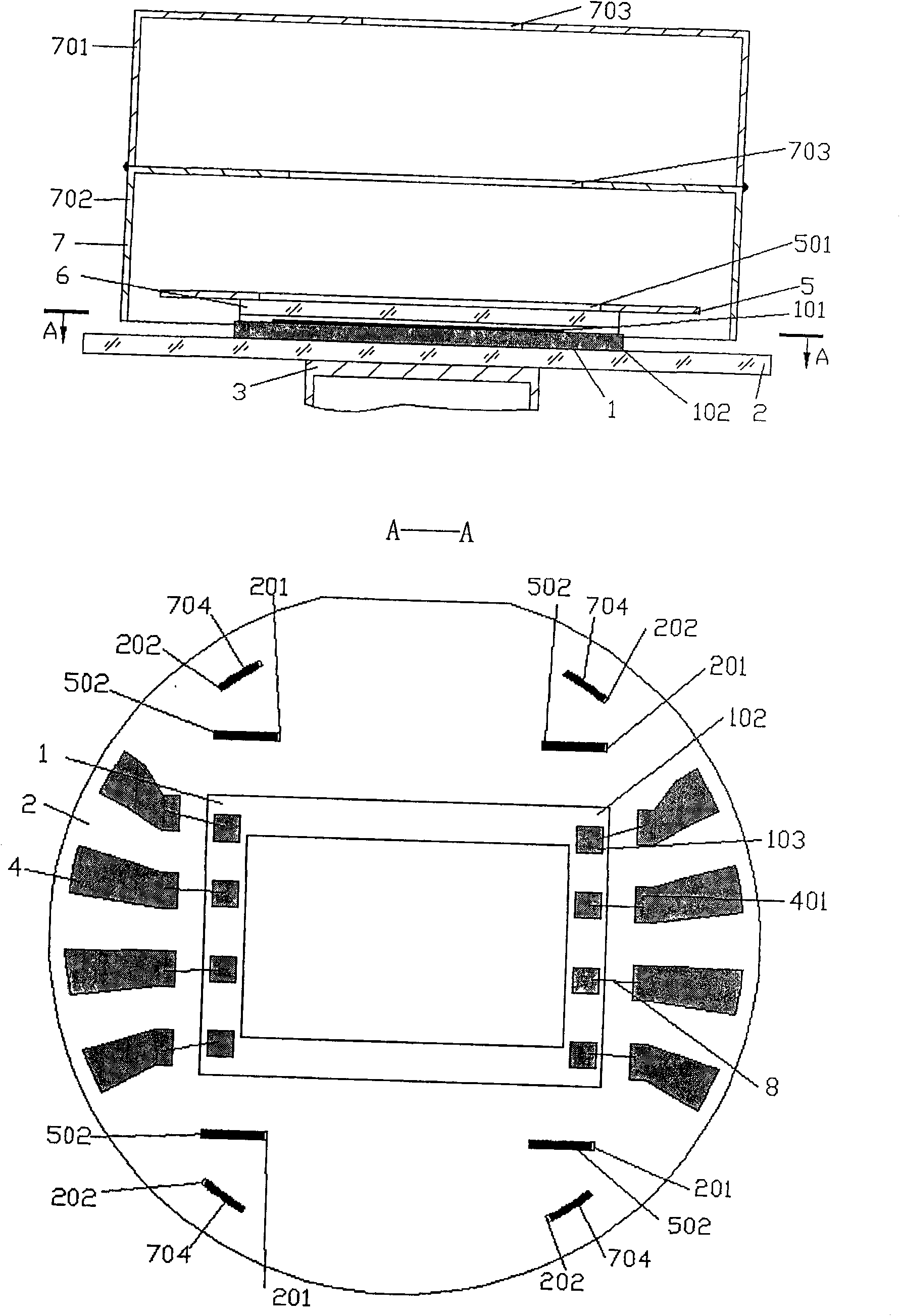
[0045] This embodiment is an assembly structure of a 320×240 area array infrared detector on a cold platform, as attached figure 1 As shown, its main implementation method is as follows:

[0046] (1) The photosensitive element 101 and the readout circuit module 102 are directly flip-bonded to form the infrared detector chip 1 . The circuit lead-out terminals 103 of the readout circuit 102 are arranged on both side edges of the readout circuit module 102 .

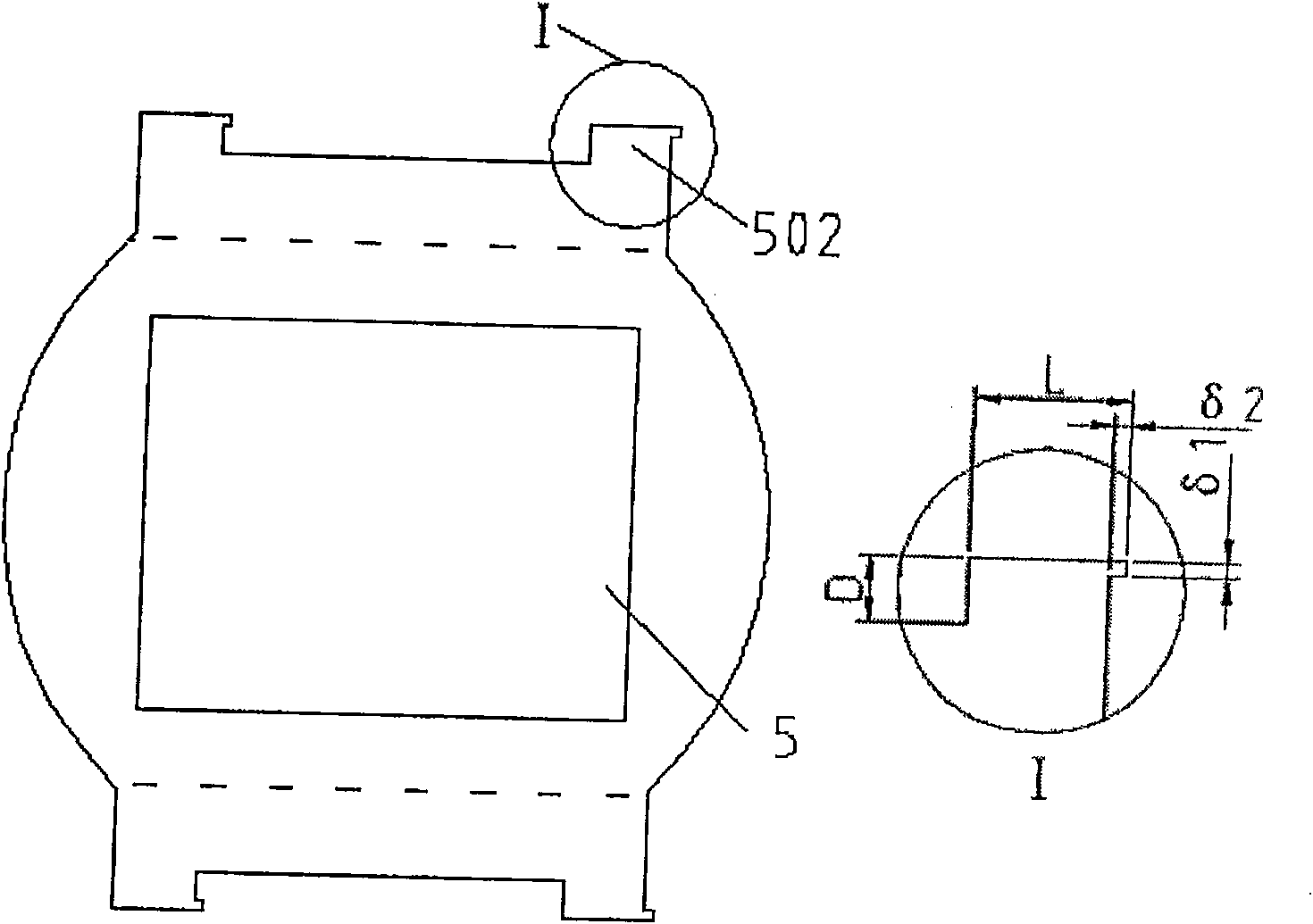
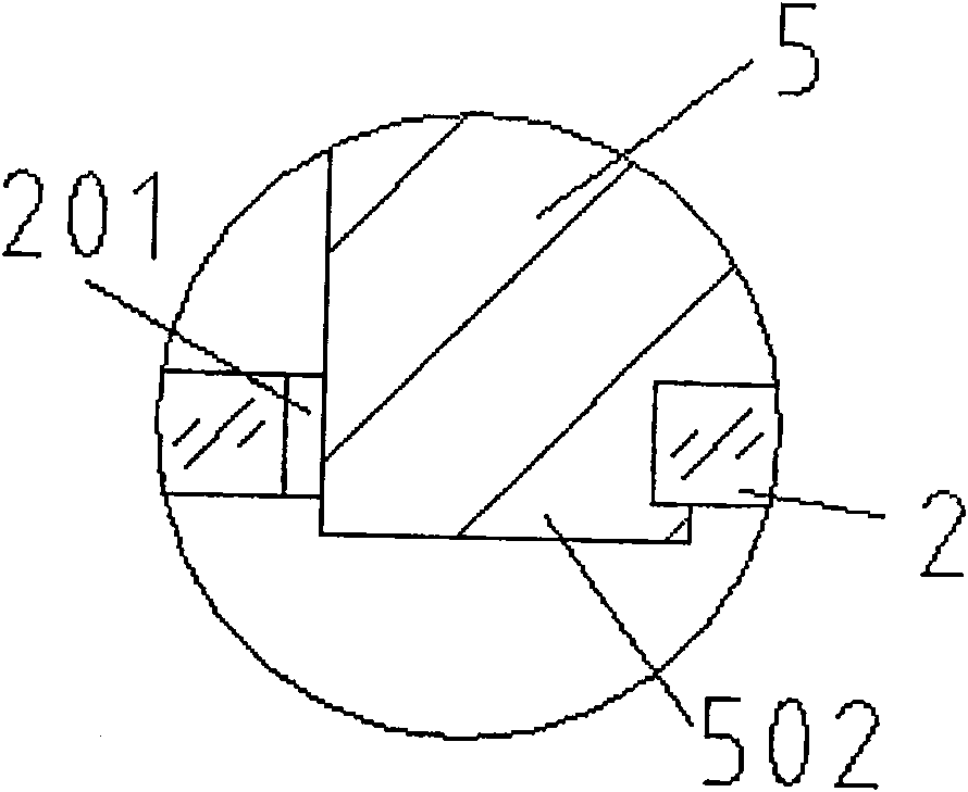
[0047] (2) Substrate The substrate 2 is a sapphire sheet with a thickness of ф21.7mm and a thickness of 0.6mm. On the ф21.7mm round gemstone after cleaning, ion-sputter a Cr film with a thickness of 300A, and then sputter Au to make the thickness of the metal layer reach 1μm, and then photoetch and corrode the designed lead circuit pattern on the gemstone. Lead circui...


PUM


Abstract

The invention discloses an assembly structure of a big area array infrared focal plane detector in a cold platform and a composition method, which is applicable to seal a Dewar of a big area array infrared focal plane detector chip. The assembly structure of the big area array infrared focal plane detector in the cold platform comprises a big area array infrared detector chip, a substrate, the cold platform of a micro-type Dewar, a lead wire circuit, a filter bracket, a filter, a thermal shield and a silicon-aluminum wire, wherein the thermal shield comprises two types of common cylinders. Through a specific treatment method that the substrate, the filter bracket and the cold platform are prepared and led, and the assembly structure of the big area array infrared focal plane detector in the cold platform is achieved. The invention reduces the heat capacity of the cold platform of the micro-type Dewar, reduces the cooling time, simultaneously effectively inhibits stray light and reducesthe parasitic thermal load of a micro-type Dewar composition.

Description

technical field [0001] The invention relates to an infrared detector chip packaging technology, specifically an assembly structure and an assembly method of a large area array infrared focal plane detector on a micro Dewar cold platform, which is suitable for a large area array infrared focal plane detector chip Micro Dewar package. Background technique [0002] High spatial resolution infrared remote sensing instrument is the core component of infrared early warning, search and tracking system. There are generally two ways to improve the spatial resolution. One is to improve the photoelectric performance of infrared detectors and improve detection sensitivity to obtain more information; the other is to increase the number of infrared sensitive elements, that is, remote sensing instruments at the same height and the same swath , the more sensitive elements, the higher the spatial resolution. Therefore, the preparation technology of large area array infrared focal plane com...

Claims


Application Information

Patent Timeline
Patent Type & Authority Patents(China)
IPC IPC(8): H01L25/00H01L23/488H01L23/49
CPCH01L2924/0002
Inventor 王小坤朱三根张亚妮曾智江郝振贻吴家荣洪斯敏俞君龚海梅
Owner SHANGHAI INST OF TECHNICAL PHYSICS - CHINESE ACAD OF SCI
Why Eureka
Try Eureka