Method of producing ceramic green sheet and electronic component

A manufacturing method and technology of ceramic green sheets, which are applied in coil manufacturing, manufacturing tools, ceramic molding machines, etc., can solve problems such as uneven electrical characteristics, differences in substrate height, formation accuracy and formation position of concave parts, and achieve basic Improved sheet thickness controllability, reduced unevenness in electrical properties, and excellent thickness uniformity

Inactive Publication Date: 2010-01-13
TDK CORPARATION
View PDF9 Cites 0 Cited by
  • Summary
  • Abstract
  • Description
  • Claims
  • Application Information

AI Technical Summary

Problems solved by technology

[0012] Therefore, when screen printing is performed to embed the conductive paste in the concave portion, the concave portion may be deformed, causing problems in the formation accuracy and formation position of the concave portion.
Therefore, in fact, it is difficult to make the formation accuracy of the concave portion and the electrode formation accuracy by screen printing consistent, and due to the difference in their positional accuracy or the positional deviation when each is formed, there may be a difference in height or height on the substrate. gap
Furthermore, the existence of the convex portion promotes the occurrence of the difference in molding density during lamination pressurization as described in Patent Document 2.
Therefore, it is considered that even if the occurrence of the difference in height is suppressed to some extent, the above-mentioned unevenness in the electrical characteristics will still occur.

Method used


Image

  • Method of producing ceramic green sheet and electronic component
  • Method of producing ceramic green sheet and electronic component
  • Method of producing ceramic green sheet and electronic component

Examples


Embodiment Construction

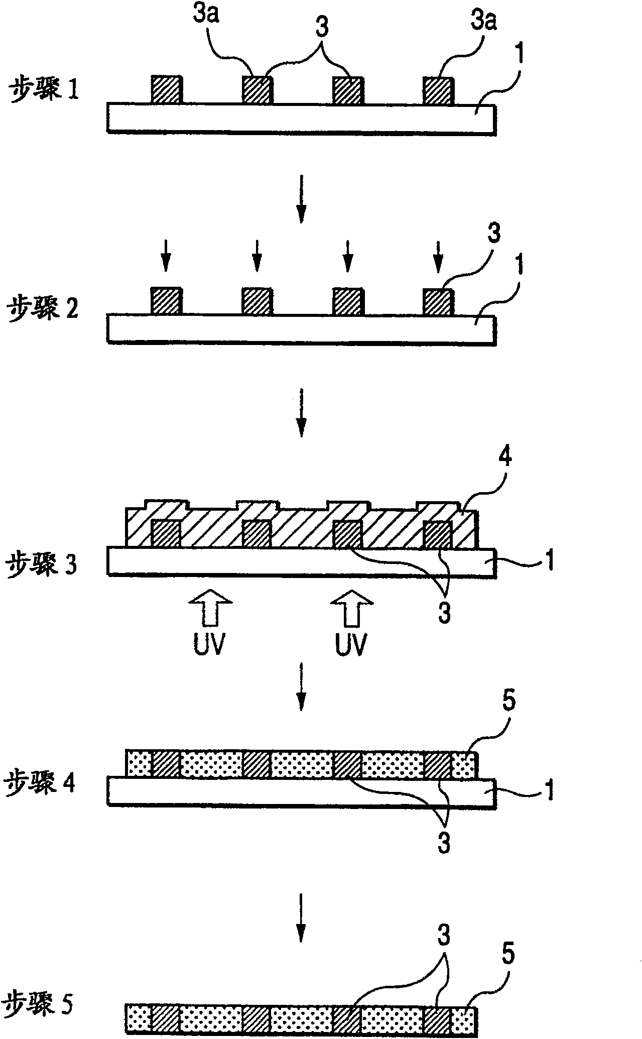
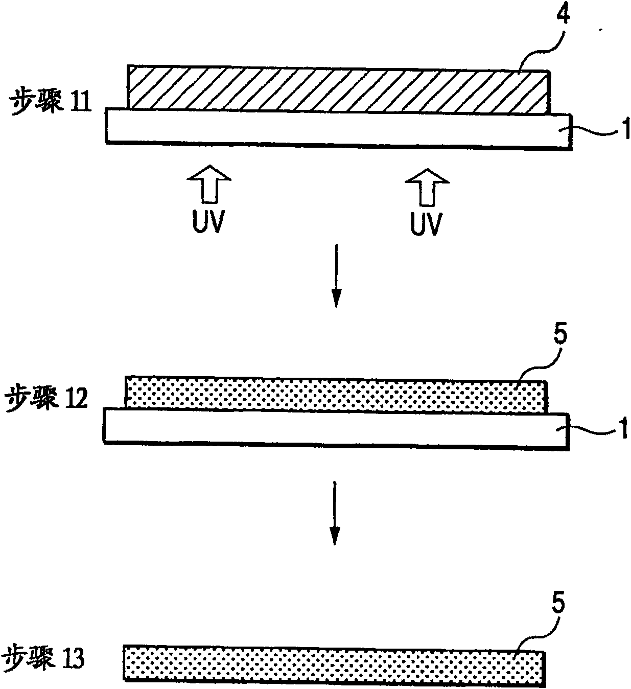
[0047] Hereinafter, embodiments of the present invention will be described in detail with reference to the drawings. figure 1 Regarding the method of manufacturing an electronic component according to the embodiment of the present invention, a method of forming a single layer of a ceramic green sheet including an electrode portion is shown. In the drawings, the cross-sections of the substrates in the respective steps are shown, and the steps are carried out according to the arrows. In the accompanying drawings, the substrate 1 is, for example, a PET film whose surface has undergone appropriate mold release treatment using transparent silicone resin or the like. Furthermore, for example, by screen printing, in step 1, the electrode portion 3 is formed on the surface of the substrate 1 subjected to the release treatment using a conductive paste conventionally used for forming electrodes. The electrode portion is formed of a light-shielding portion made of a material that does n...


PUM

PropertyMeasurementUnit
thicknessaaaaaaaaaa
thicknessaaaaaaaaaa
diameteraaaaaaaaaa

Abstract

A laminated ceramic electronic component, wherein a ceramic green sheet used for forming this has an internal electrode and is flat. Specifically, a ceramic green sheet is obtained by forming electrode parts on the surface of a transparent substrate, spreading thereover photosensitive slurry having dielectric powder, exposing this photosensitive slurry up to a specified thickness from the rear surface of the substrate and then developing this, and later removing the substrate.

Description

technical field [0001] The present invention relates to a method of manufacturing an electronic device, particularly a so-called multilayer ceramic formed by laminating ceramics, and a method of manufacturing a so-called ceramic green sheet used therein. In addition, as the multilayer ceramic electronic components described here, multilayer ceramic capacitors, multilayer ceramic inductors, and LC composite components incorporating them or EMC-related components will be described as specific examples. Background technique [0002] In recent years, with the miniaturization and rapid spread of electronic equipment such as mobile phones, people are also seeking to achieve higher density mounting and high performance of electronic components used in them. In particular, multilayer ceramic electronic components used as passive devices are required to be thinner, multilayered, and uniform in each layer in order to meet such requirements, and research is being conducted on manufactu...

Claims


Application Information

Patent Timeline
Patent Type & Authority Patents(China)
IPC IPC(8): H01G4/12H01G4/30H01F41/04B28B1/30B28B1/00B28B11/00B28B11/24
Inventor 吉田政幸须藤纯一青木俊二渡边源一
Owner TDK CORPARATION
Why Eureka
Try Eureka