Method of manufacturing metal oxide semiconductor device

A technology of oxide semiconductor and manufacturing method, applied in semiconductor/solid-state device manufacturing, semiconductor devices, electrical components and other directions, can solve the problems of high cost and low production efficiency, and achieve the effect of low manufacturing cost, improving efficiency and reducing cost

Active Publication Date: 2009-12-30
SEMICON MFG INT (SHANGHAI) CORP +1
View PDF4 Cites 0 Cited by
  • Summary
  • Abstract
  • Description
  • Claims
  • Application Information

AI Technical Summary

Problems solved by technology

However, the ion implantation process uses ion beam scanning for ion implantation, so there are defects of low production efficiency and high cost.

Method used


Image

  • Method of manufacturing metal oxide semiconductor device
  • Method of manufacturing metal oxide semiconductor device
  • Method of manufacturing metal oxide semiconductor device

Examples


Embodiment Construction

[0027] In order to make the above objects, features and advantages of the present invention more comprehensible, specific implementations of the present invention will be described in detail below in conjunction with the accompanying drawings.

[0028] In the following description, numerous specific details are set forth in order to provide a thorough understanding of the present invention. However, the present invention can be implemented in many ways other than those described here, and those skilled in the art can make similar extensions without departing from the connotation of the present invention. Accordingly, the invention is not limited to the specific implementations disclosed below.

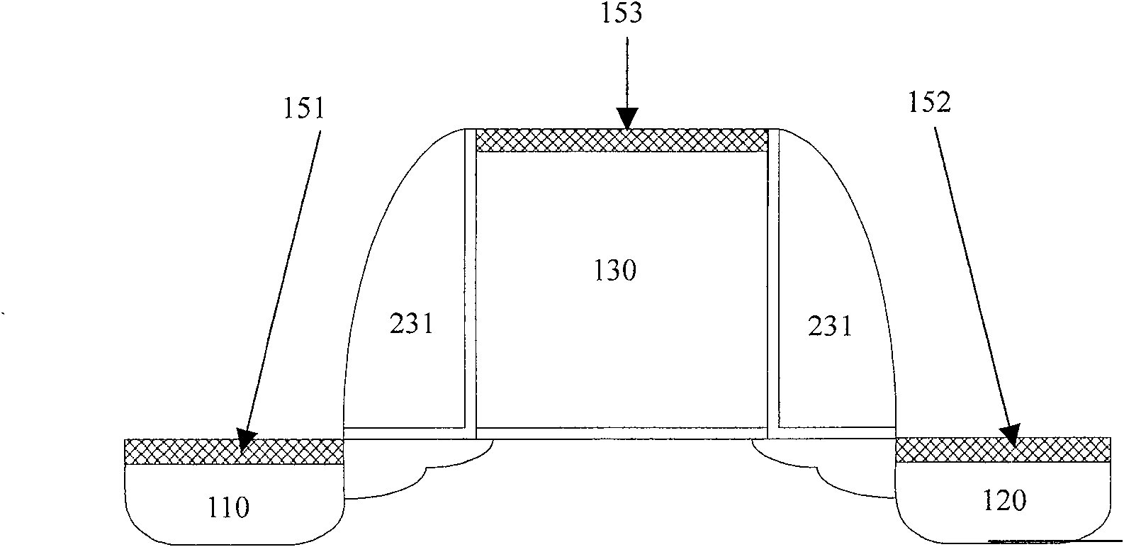
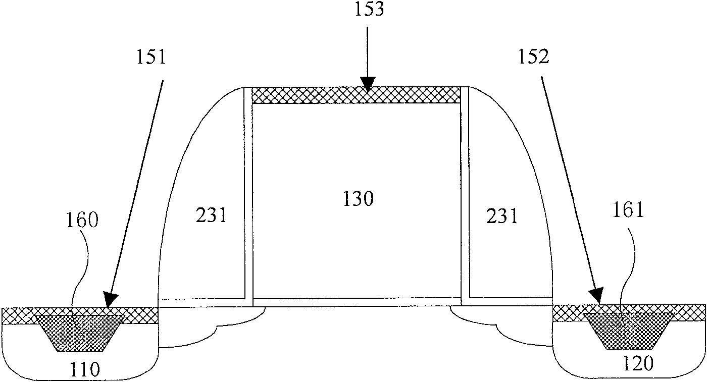
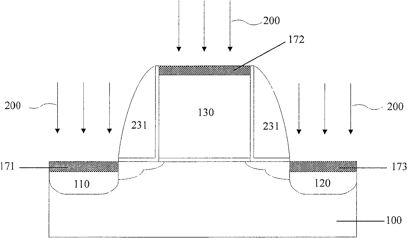
[0029] The method for manufacturing metal oxide semiconductor devices provided by the present invention is suitable for manufacturing semiconductor devices with a feature size of 65nm or below. The semiconductor device is not only a MOS transistor, but also includes a PMOS transistor ...


PUM

PropertyMeasurementUnit
widthaaaaaaaaaa

Abstract

The invention discloses a method of manufacturing a metal oxicide semiconductor device which comprises the following steps of: forming a grid, a source region and a drain region on a semiconductor substrate wherein, the two sides of the grid are provided with sidewall spacers; implanting plasma into the grid, the source region and the drain region which achieves non-crystallization of the surface; depositing metals on the surface of the grid, the source region and the drain region; thermal annealing the metal to form a metal silicide layer. The method of the invention can form a barrier layer by an efficient method and the risk of forming sprinkling in the S / D region can be reduced and the production cost can also be reduced.

Description

technical field [0001] The invention relates to the technical field of semiconductor manufacturing, in particular to a method for manufacturing metal oxide semiconductor (MOS) devices. Background technique [0002] In order to reduce the sheet resistance and parasitic resistance of source / drain electrodes and gates of MOS transistors in ultra-high-speed large-scale integrated circuits, a self-aligned silicide (salicide) process is used. In the self-alignment technology, the reaction product of metal and semiconductor such as silicon (Si), that is, silicide (hereinafter referred to as metal silicide). Metal suicide plays a very important role in VLS / ULSI device technology. In MOS devices, metal silicides are often used to obtain good low resistance contacts. Metal silicides can be used to provide contact surfaces between metal lines and substrate contact areas, such as polysilicon gates, sources and drains on silicon substrates. figure 1 It is a schematic diagram of the p...

Claims


Application Information

Patent Timeline
Patent Type & Authority Patents(China)
IPC IPC(8): H01L21/336H01L21/28H01L21/265
Inventor 吴汉明
Owner SEMICON MFG INT (SHANGHAI) CORP
Why Eureka
Try Eureka