
Production of multi-layer circuit board of built-in passive assembly

A technology of multi-layer circuit boards and passive components, which can be used in the manufacture of multi-layer circuits and the assembly of printed circuits with electrical components, which can solve the problems of poor electrical accuracy and complex processes.

Active Publication Date: 2009-05-20
ADVANCED SEMICON ENG INC
View PDF5 Cites 0 Cited by
  • Summary
  • Abstract
  • Description
  • Claims
  • Application Information

AI Technical Summary

Problems solved by technology

[0004] However, the above method must consider the process performance of resistors or capacitors. For example, the printed area of ​​resistor materials needs to be carefully controlled to avoid problems such as poor electrical accuracy caused by differences between the printed resistors and the original design values. Therefore, the overall The process will be more complicated

Method used


Image

  • Production of multi-layer circuit board of built-in passive assembly
  • Production of multi-layer circuit board of built-in passive assembly
  • Production of multi-layer circuit board of built-in passive assembly

Examples


Embodiment Construction

[0041] Specific embodiments of the present invention will be described in detail below in conjunction with the accompanying drawings.

[0042] The following icons are for simple illustration only, and are not drawn according to the actual size, that is, they do not reflect the actual size and characteristics of each layer in the multilayer circuit board structure.

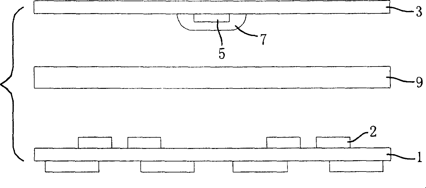
[0043] see Figure 2A to Figure 2E , a cross-sectional view of the manufacturing process of the first preferred embodiment of the multilayer circuit board with embedded passive components of the present invention.

[0044] like Figure 2A As shown, a single-layer board is firstly provided, the single-layer board includes a dielectric layer 10 and a first conductive foil 12, the dielectric layer 10 has a first surface 11a and a second surface 11b, and the first conductive foil 12 is arranged on the first on the surface 11a.

[0045] The material of the dielectric layer 10 is an insulating material, which may be a...


PUM


Abstract

The method comprises: providing a single layer board comprising a dielectric layer and a first conducting foil; the dielectric layer has a first surface and a second surface, and the first conducting layer is located on the first surface; heating up the single layer board to melt the dielectric layer; pressing a passive element into the melted dielectric layer from the second surface; overlapping the single layer board on a core board; overlapping a second conducting foil on the single layer board, and forming a circuit pattern on the second conducting foil.

Description

technical field [0001] The invention relates to a method for manufacturing a multilayer circuit board, in particular to a method for manufacturing a multilayer circuit board with embedded passive components. Background technique [0002] In order to further create more space and improve the versatility of the module in a limited substrate area, active components (active components) are often constructed by reducing or embedding passive components (passive components) to create more space. ), and then developed a multi-layer circuit board embedded with passive components, such as resistors, capacitors, inductors, and voltage-controlled quartz oscillators. [0003] There are many methods that can be used to integrate a variety of film-like passive components in a multilayer circuit board, but for the multilayer circuit board process, the key is the ability of the circuit board to embed such thick film or thin film passive components. Process performance, that is, how to maint...

Claims


Application Information

Patent Timeline
Patent Type & Authority Patents(China)
IPC IPC(8): H05K3/46H05K3/30
Inventor 洪清富王永辉
Owner ADVANCED SEMICON ENG INC
Learn More