


Quick Research
Generate reliable direction feasibility study reports for your R&D in just a few steps.

Technical Q&A
Discover and master advanced knowledge NOW. Basics, ideas, possibilities, all at once.

Find Solutions
As an expert in R&D theories, this can generate solutions to your technical problems instantly.

Evaluate Feasibility
Analyze your overall solution with one click, know your potential R&D risks in advance.

Monitor Landscape
Get weekly tech updates, stay abreast of the latest tech innovations and key insights.
Method for forming solder pad of semiconductor device
A semiconductor and device technology, applied in the field of semiconductor device pad formation, can solve the problems of long processing time of organic solvents and limiting production capacity, and achieve the effects of preventing electrochemical corrosion, improving production capacity, and reducing processing time
- Summary
- Abstract
- Description
- Claims
- Application Information
AI Technical Summary
Problems solved by technology
Method used
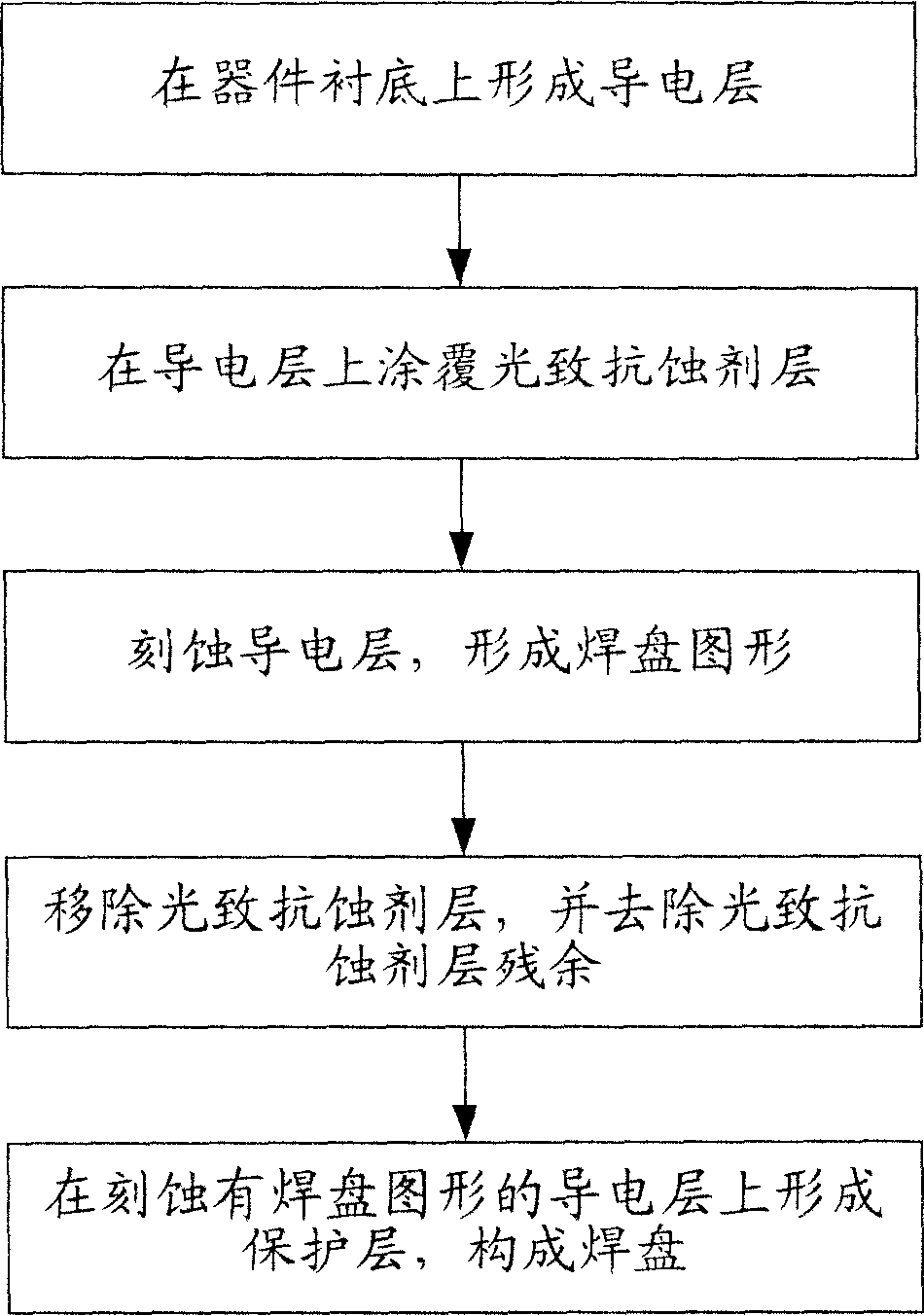
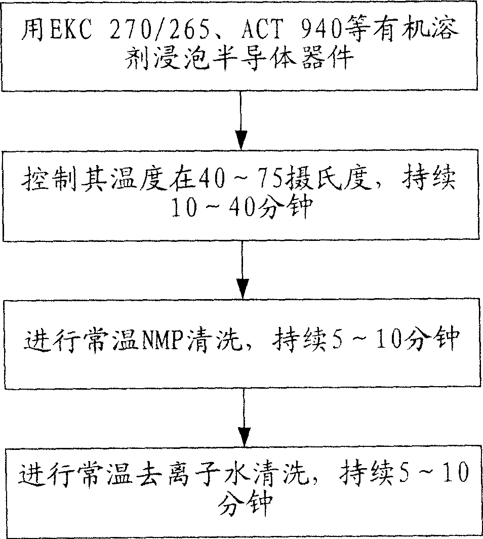
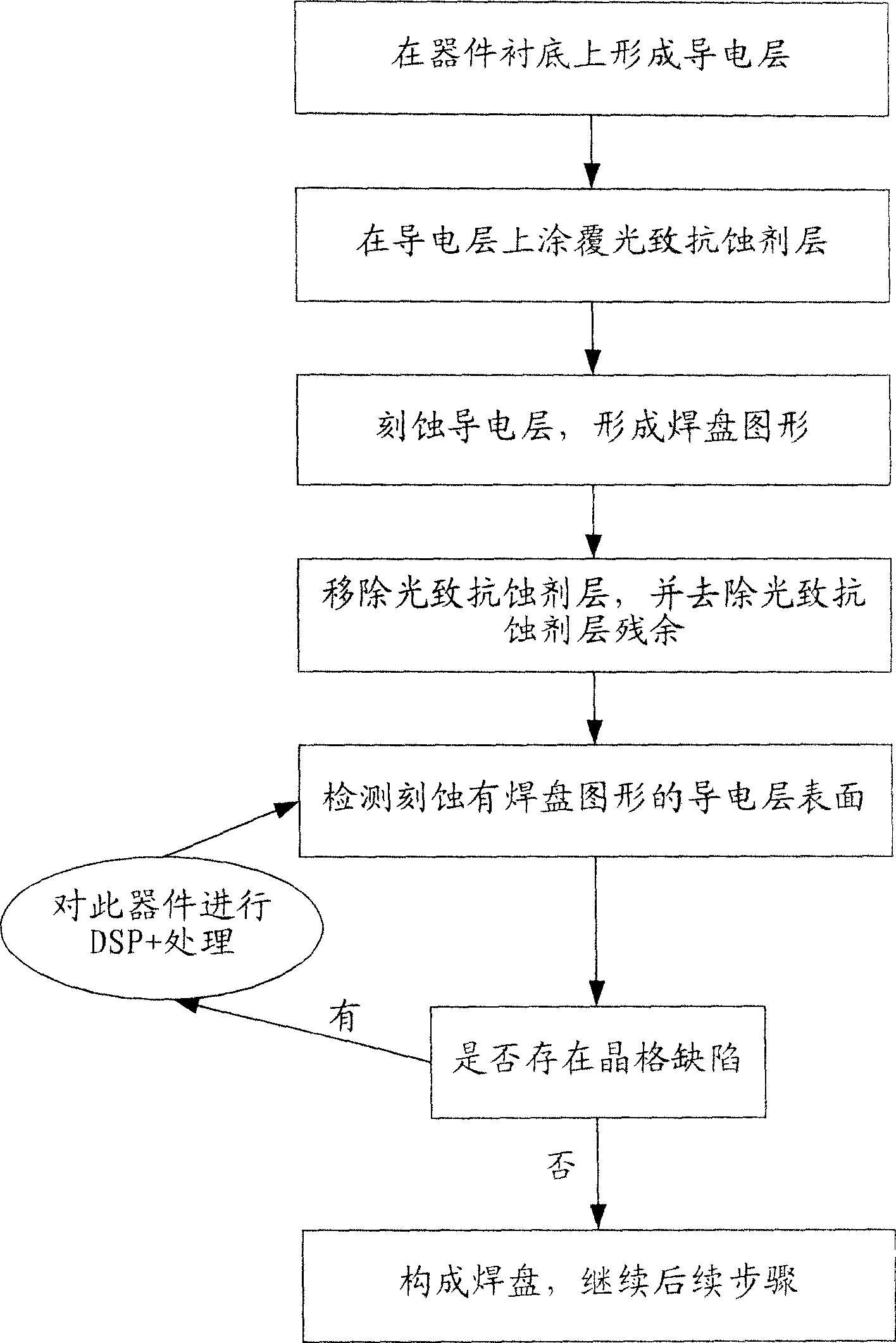
Image

Examples
Embodiment Construction
[0028] Although the present invention will be described in more detail below with reference to the accompanying drawings, in which preferred embodiments of the invention are shown, it should be understood that those skilled in the art can modify the invention described herein and still achieve the advantageous effects of the invention. Therefore, the following description should be construed as a broad teaching for those skilled in the art, rather than as a limitation of the present invention.
[0029] In the interest of clarity, not all features of an actual embodiment are described. In the following description, well-known functions or constructions are not described in detail since they would obscure the invention with unnecessary detail. It should be recognized that in the development of any actual embodiment, a number of implementation details must be made to achieve the developer's specific goals, such as changing from one embodiment to another in accordance with system-...
PUM
 Abstract
Description
Claims
Application Information
 - R&D Engineer
- R&D Manager
- IP Professional
- Industry Leading Data Capabilities
- Powerful AI technology
- Patent DNA Extraction
Browse by: Latest US Patents, China's latest patents, Technical Efficacy Thesaurus, Application Domain, Technology Topic, Popular Technical Reports.
© 2024 PatSnap. All rights reserved.Legal|Privacy policy|Modern Slavery Act Transparency Statement|Sitemap|About US| Contact US: help@patsnap.com