Chip packaging structure and manufacturing method therefor

A technology of chip packaging and manufacturing methods, applied in semiconductor/solid-state device manufacturing, electrical components, electrical solid-state devices, etc., can solve problems such as electrical short circuit, electrical open circuit, and the third bonding wire 150 is easy to collapse, so as to improve reliability Degree, the effect of improving production yield

Inactive Publication Date: 2009-02-18
CHIPMOS TECHSHANGHAI +1
View PDF3 Cites 0 Cited by
  • Summary
  • Abstract
  • Description
  • Claims
  • Application Information

AI Technical Summary

Problems solved by technology

Therefore, the length of these third welding wires 150 is relatively long, so that these third welding wires 150 are easy to collapse and cause an electrical short circuit.
Or, these third welding wires 150 are prone to collapse or be torn off by the poured glue during sealing, resulting in electrical disconnection

Method used


Image

  • Chip packaging structure and manufacturing method therefor
  • Chip packaging structure and manufacturing method therefor
  • Chip packaging structure and manufacturing method therefor

Examples


no. 1 example

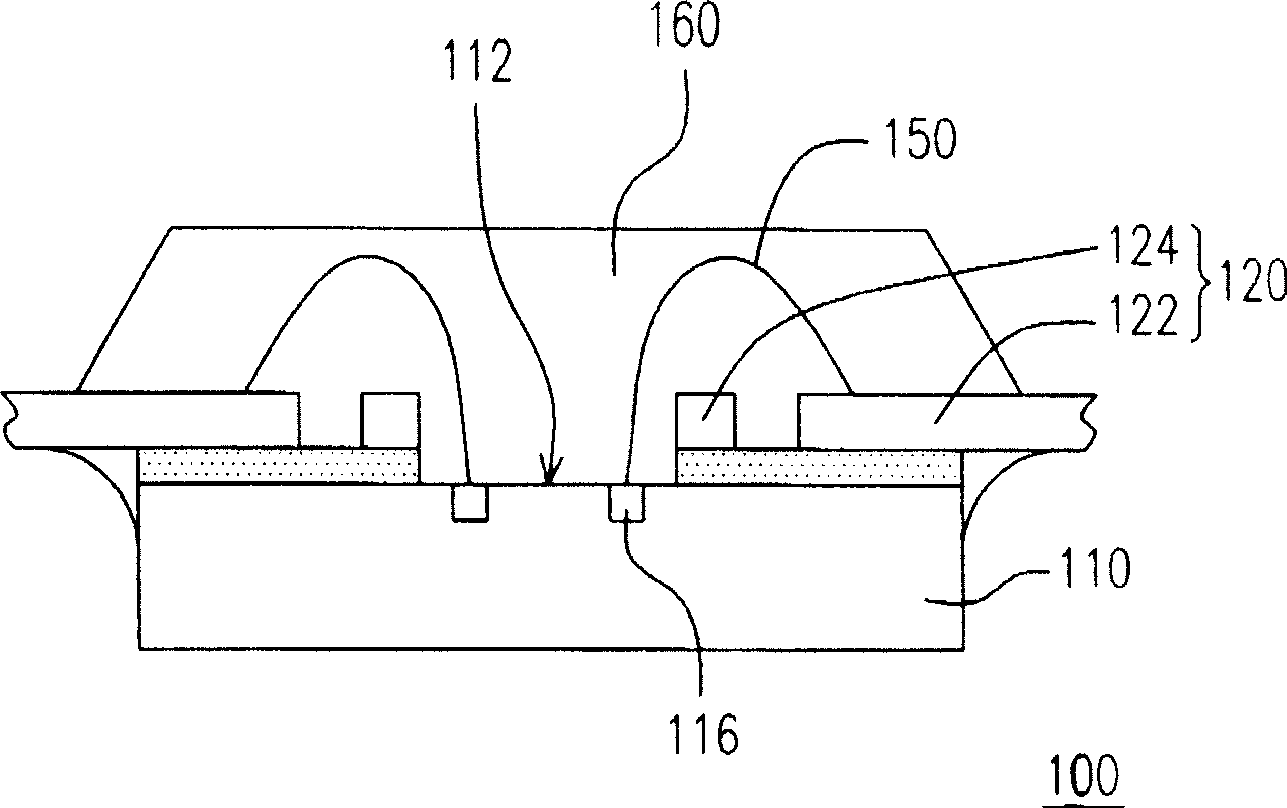
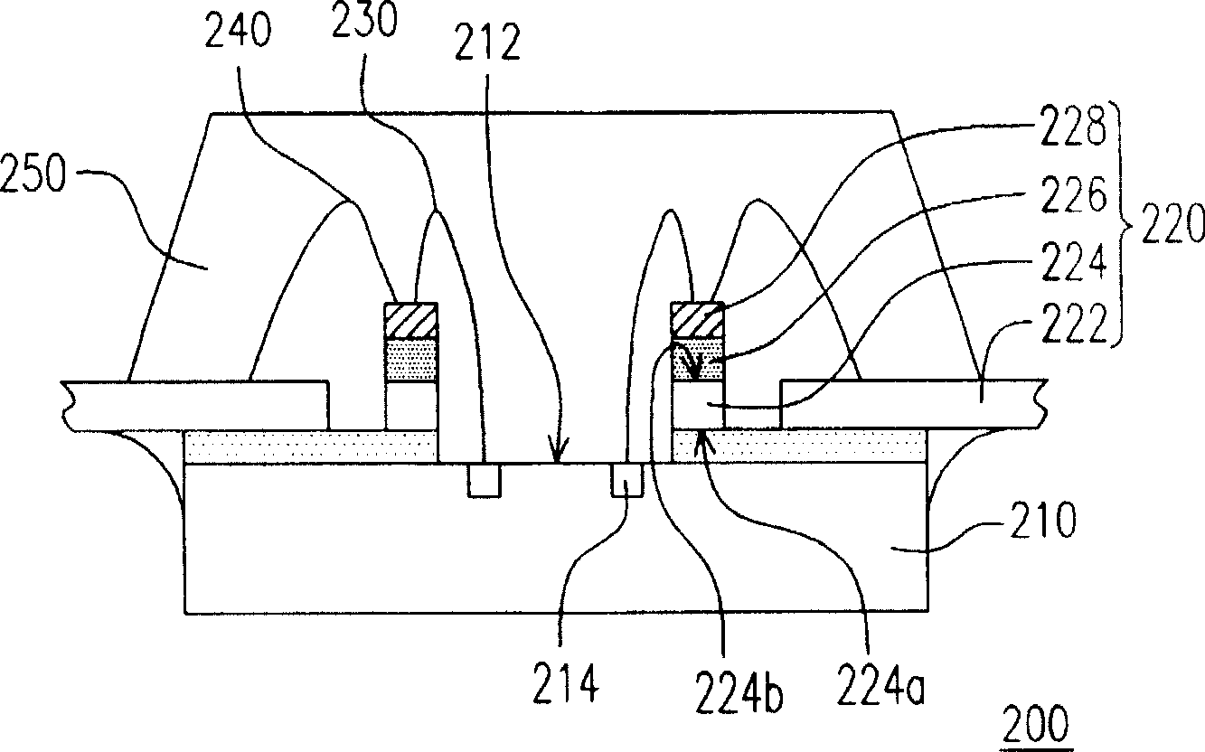
[0053] Figure 2A A schematic side view sectional view of a chip package structure according to the first embodiment of the present invention is shown, and Figure 2B draw Figure 2A A schematic top view of the lead frame of the chip package structure. Please refer to Figure 2A and Figure 2B The chip package structure 200 of the first embodiment includes a chip 210 , a lead frame 220 , a plurality of first bonding wires 230 and a plurality of second bonding wires 240 . The chip 210 has an active surface 212 and a plurality of chip pads 214 , wherein the chip pads 214 are disposed on the active surface 212 . In addition, these chip pads 214 can be ground pads, power pads or signal pads.

[0054] The lead frame 220 is fixed on the chip 210 , and the lead frame 220 includes a plurality of inner leads 222 , at least one bus frame 224 , an insulating layer 226 and a plurality of transfer pads 228 . The bus frame 224 is located between the chip pads 214 and the inner pins 22...

no. 2 example

[0064] Figure 4A A schematic side sectional view of a chip package structure according to the second embodiment of the present invention is shown, and Figure 4B draw Figure 4A A schematic top view of the lead frame of the chip package structure. Please refer to Figure 4A and Figure 4B The main difference between the chip package structure 300 of the second embodiment and the chip package structure 200 of the first embodiment is that: the lead frame 320 of the chip package structure 300 includes a chip seat P, a plurality of inner pins 322, at least— The bus frame 324 , an insulating layer 326 and a plurality of transfer pads 328 . The wafer 310 is disposed on the wafer seat P, and the active surface 312 is away from the wafer seat P. As shown in FIG. In other words, just Figure 4A In terms of relative position, the active surface 312 of the wafer 310 is facing upward. In addition, the busbar 324 is located between the wafer pad P and the inner pins 322 .

[0065]...


PUM


Abstract

The present invention relates to a wafer packaging structure, which comprises a wafer, a lead frame, a plurality of first welding lines and a plurality of second welding lines. The wafer is provided with an active face and a plurality of wafer welding mats positioned on the active face. The lead frame fixedly positioned on the wafer comprises a plurality of pins, at least one flow concentration frame, an insulating layer and a plurality of shifting welding mats. The flow concentration frame is arranged between the wafer welding mats and the inner pins. The insulating layer is positioned on the flow concentration frame. The shifting welding mat is positioned on the insulating layer, and the inner pins and the flow concentration frame are arranged above the active face, and the wafer and the insulating layer are respectively arranged on the two surfaces face to face of the flow concentration frame. The first welding lines are respectively connected with the wafer welding mats and the shifting welding mats, and the second welding lines are respectively connected with the shifting welding plate and the inner pins. The wafer packaging structure can reduce the falling possibility of the welding line.

Description

technical field [0001] The present invention relates to a semiconductor element and its manufacturing method, and in particular to a chip packaging structure and its manufacturing method (CHIP PACKAGE AND MANUFACTURING METHODTHREROF). Background technique [0002] In the semiconductor industry, the production of integrated circuits (IC) can be mainly divided into three stages: integrated circuit design (IC design), integrated circuit manufacturing (IC process) and integrated circuit packaging (IC package). [0003] In the fabrication of integrated circuits, a chip is completed through wafer fabrication, integrated circuit formation, and wafer sawing. The wafer has an active surface, which generally refers to the surface of the wafer with active devices. After the integrated circuit inside the wafer is completed, the active surface of the wafer is further equipped with a plurality of bonding pads, so that the chip finally formed by dicing the wafer can be electrically connec...

Claims


Application Information

Patent Timeline
Patent Type & Authority Patents(China)
IPC IPC(8): H01L23/495H01L21/60
CPCH01L2224/4826H01L2224/48091H01L2224/73265H01L2224/32245H01L2924/19107H01L2224/73215H01L2924/00014H01L2924/00
Inventor 潘华邱介宏黄志龙
Owner CHIPMOS TECHSHANGHAI
Why Eureka
Try Eureka