Manufacturing method for chromatic filter layer

A technology for a color filter layer and a manufacturing method, which is applied in semiconductor/solid-state device manufacturing, optics, nonlinear optics, etc., can solve the problems such as difficulty in adjusting the alignment accuracy of the color filter layer, decrease in panel light transmittance, and the like. Aperture ratio, effect of reducing manufacturing cost

Active Publication Date: 2008-12-31
AU OPTRONICS CORP
View PDF4 Cites 1 Cited by
  • Summary
  • Abstract
  • Description
  • Claims
  • Application Information

AI Technical Summary

Problems solved by technology

However, the above-mentioned parameters that affect brightness can be improved by materials or design, but the assembly accuracy of the color filter layer and the alignment accuracy of the black matrix are still limited by the capabilities of the equipment and difficult to adjust, resulting in panel transparency. light rate drop

Method used


Image

  • Manufacturing method for chromatic filter layer
  • Manufacturing method for chromatic filter layer
  • Manufacturing method for chromatic filter layer

Examples


Embodiment Construction

[0056] In order to make the above and other objects, features and advantages of the present invention more comprehensible, preferred embodiments are described below in detail with accompanying drawings.

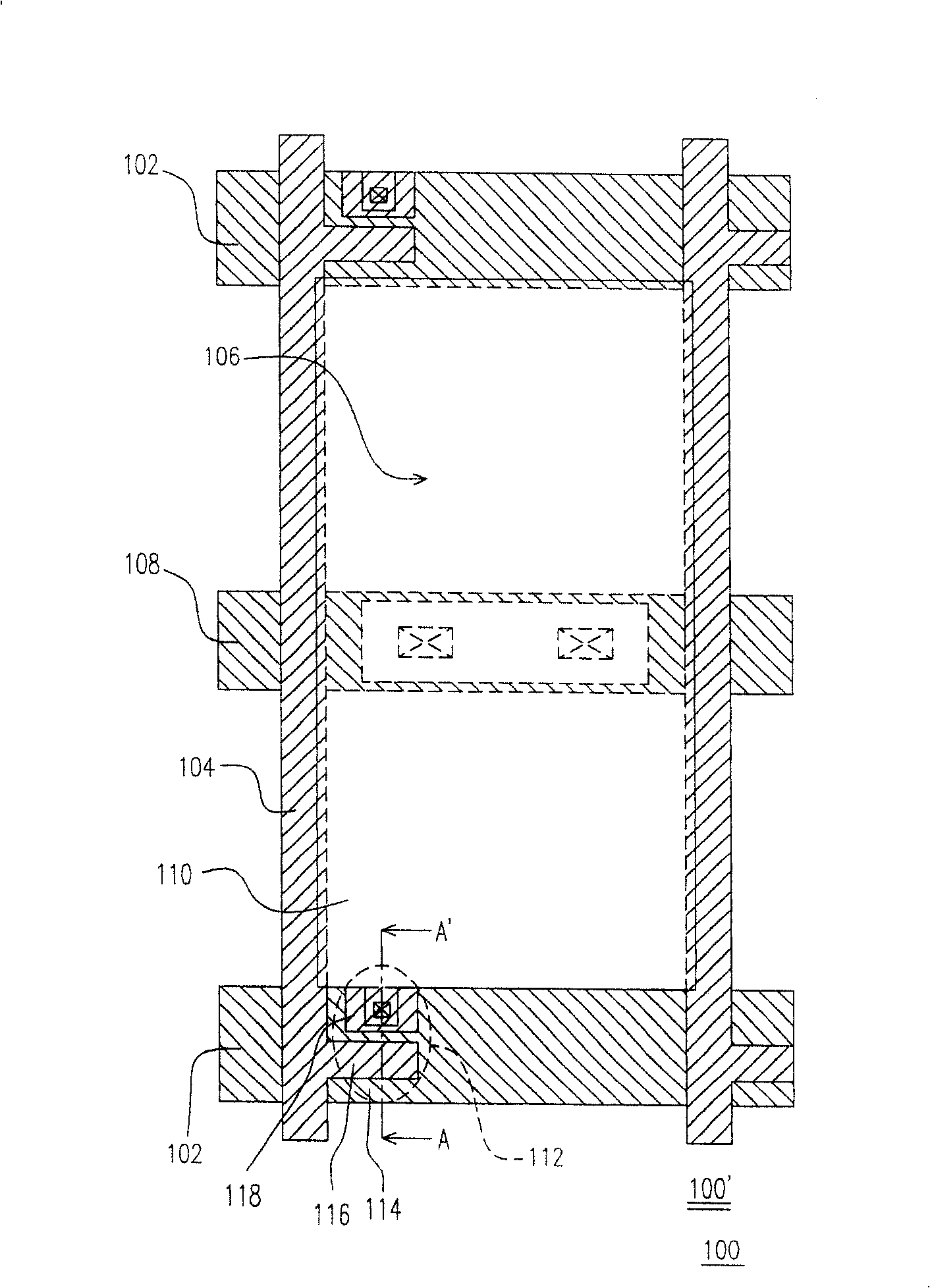
[0057] Figure 1A , Figure 1B What is shown is a top view of the manufacturing process of the color filter layer according to an embodiment of the present invention.

[0058] First, please refer to Figure 1A, providing an active component array substrate 100, such as a thin film transistor array substrate. In the active device array substrate 100, a plurality of scanning wires 102 and a plurality of data wires 104 on the substrate 100' form a plurality of pixel regions 106, and a shared wire 108 passes through the pixel region 106, and a pixel electrode 110 is located in the pixel region. In 106 , the thin film transistor 112 is located at the intersection of the scan wire 102 and the data wire 104 . In this embodiment, the opaque metal pattern can be formed by metal patt...


PUM


Abstract

The invention provides a color filter layer manufacturing method, the method including: provide an active component array substrate, the active component array substrate having the opaque metal pattern; and subsequently, use the opaque metal pattern as a mask, using the back exposure mode to form a black matrix in the active component array substrate, and the black matrix defines a number of pixel areas; then, in the said pixel area, forming a number of color filter patterns. The color filter layer manufacturing method of this invention can produce the black matrix with no contraposition error, thus contributing to produce the panel without color filter layer group deviation, and using the color filter layer manufacturing method of the invention can save the use of masks, which will reduce the manufacturing cost of panels, and in addition, the color filter layer manufacturing method of the invention contributes to produce high opening rate panels.

Description

technical field [0001] The present invention relates to a method for manufacturing a color filter layer (METHOD FORFABRICATING COLOR FILTER LAYER), and in particular to a method for manufacturing a color filter layer without alignment errors. Background technique [0002] Cathode Ray Tube (CRT) has been monopolizing the display market in recent years due to its excellent display quality and economy. However, for the environment where individuals operate most terminal / display devices on the table, or from the perspective of environmental protection, if the trend of energy saving is predicted, there are still many problems in space utilization and energy consumption of cathode ray tubes. In terms of light, thin, short, small and low power consumption requirements, CRT cannot provide an effective solution. Therefore, thin film transistor liquid crystal displays (Thin Film Transistor Liquid Crystal Display, TFT-LCD) with superior characteristics such as high image quality, high...

Claims


Application Information

Patent Timeline
Patent Type & Authority Patents(China)
IPC IPC(8): G02F1/1335G02F1/1333G03F7/20G03F7/26G02F1/1362
Inventor 董畯豪钟瑞婴
Owner AU OPTRONICS CORP
Why Eureka
Try Eureka