


Quick Research
Generate reliable direction feasibility study reports for your R&D in just a few steps.

Technical Q&A
Discover and master advanced knowledge NOW. Basics, ideas, possibilities, all at once.

Find Solutions
As an expert in R&D theories, this can generate solutions to your technical problems instantly.

Evaluate Feasibility
Analyze your overall solution with one click, know your potential R&D risks in advance.

Monitor Landscape
Get weekly tech updates, stay abreast of the latest tech innovations and key insights.
Method for preparing transparent, electric film of non-crystalline oxide
An oxide thin film, transparent conductive technology, applied in the direction of ion implantation plating, metal material coating process, coating, etc., can solve the problem of high valence difference amorphous IMO transparent conductive oxide film, etc., to achieve high carrier Good mobility and process stability
- Summary
- Abstract
- Description
- Claims
- Application Information
AI Technical Summary
Problems solved by technology
Method used
Image

Examples
Embodiment 1
[0033] Example 1. Preparation of molybdenum-doped indium oxide target: In metal with purity of 99.99% is melted into a target, prepared by uniformly and symmetrically embedding 2wt% molybdenum wire with the same purity of 99.99%. The diameter of the target is 51mm and the thickness is 2.5mm. . The substrate is an ordinary glass slide, which is cleaned by ultrasonic waves of pure water, alcohol and acetone for 15 minutes each.
[0034] Substrate temperature: 15°C.
[0035] The distance between the target and the substrate is fixed at 35mm.
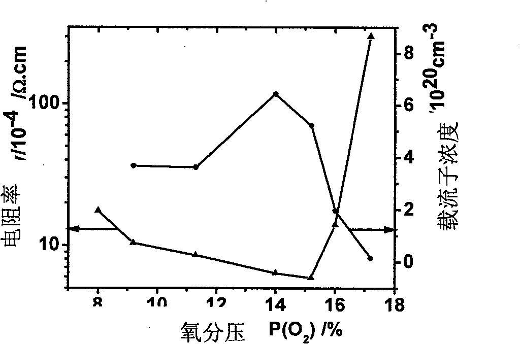
[0036] Vacuum the reaction chamber to less than 2×10 before film deposition -3 Pa, and then O 2 And Ar gas are passed into the reaction chamber. The working pressure in the reaction chamber is 2.5×10 -1 Pa, sputtering current is 100mA, sputtering voltage is 400V, control O 2 The percentage of reaction gas P(O 2 )[=PO 2 / (PO 2 +PAr)] is 8.0%. The films are all prepared on ordinary glass plates.
[0037] The sputtering time is 3 minutes, and the ...
Embodiment 2
[0038] In Example 2, an amorphous IMO film was prepared under the same method as Example 1 at a substrate temperature of 25°C under the following conditions: the sputtering current was 150mA, the sputtering voltage was 500V, and the O 2 And Ar gas into O 2 Reaction chamber and control O 2 The percentage of gas partial pressure P(O 2 ) Is 18.0%. The sputtering time is 8 minutes, and the film thickness is 160 nm.
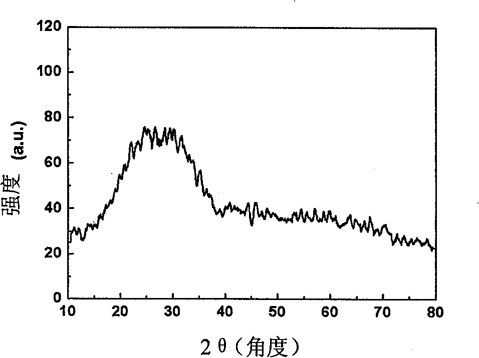
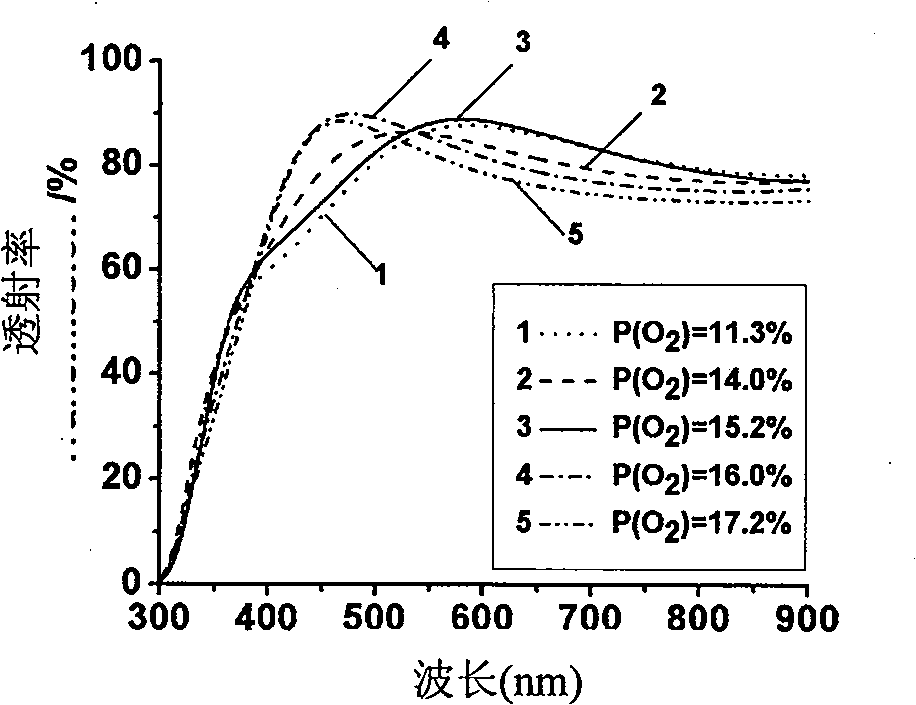
[0039] Measure the thickness d of the film with a surface profiler (Kosaka ET3000 type), and measure the sheet resistance R of the sample with a four-point probe (BD-90 type) □ , So as to calculate the resistivity ρ of the film. At room temperature, a Hall tester (Bio-Rad Microscience HL5500 Hall system) was used to measure the Hall effect of the film to obtain the carrier mobility and carrier concentration of the film. X-ray diffractometer (XRD) (Rigaku D / max-rB type, Cu Kα radiation source) is used to analyze the crystalline structure of the film; the surface of the fil...
PUM
| Property | Measurement | Unit |
|---|---|---|
| thickness | aaaaa | aaaaa |
| electrical resistivity | aaaaa | aaaaa |
| density | aaaaa | aaaaa |
Abstract
Description
Claims
Application Information
 - R&D Engineer
- R&D Manager
- IP Professional
- Industry Leading Data Capabilities
- Powerful AI technology
- Patent DNA Extraction
Browse by: Latest US Patents, China's latest patents, Technical Efficacy Thesaurus, Application Domain, Technology Topic, Popular Technical Reports.
© 2024 PatSnap. All rights reserved.Legal|Privacy policy|Modern Slavery Act Transparency Statement|Sitemap|About US| Contact US: help@patsnap.com