Semiconductor packaging with partially patterned lead frames and its making methods
A lead frame and frame technology, which is used in semiconductor/solid-state device manufacturing, semiconductor devices, and semiconductor/solid-state device components, etc., can solve problems such as low-cost lead frames, achieve uniform heat transfer, stable chip bonding processing, The effect of subsequent process safety
- Summary
- Abstract
- Description
- Claims
- Application Information
AI Technical Summary
Problems solved by technology
Method used
Image
Examples
Embodiment Construction
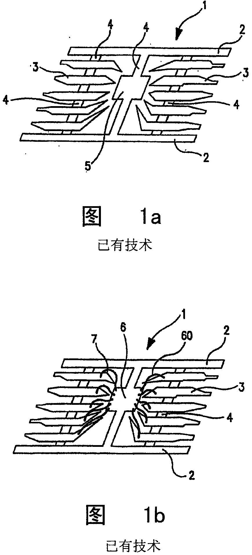
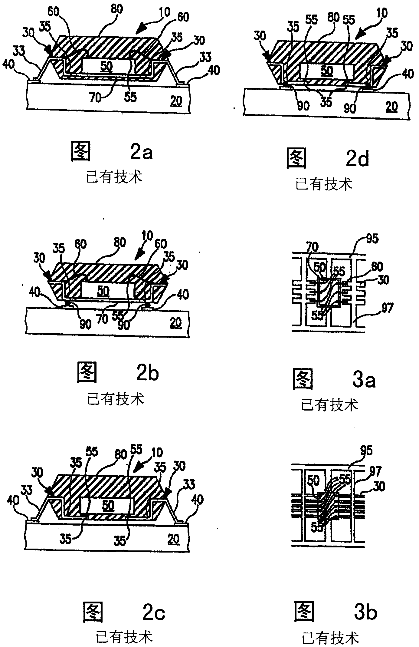
[0061] Figure 4-15band 16-24b show different embodiments for forming partially patterned leadframes that can have higher lead counts than close chip scale packages (CSPs). The method of the invention improves the automation of the production line and the quality and reliability of the packages produced thereby. This is accomplished by performing most of the manufacturing process steps and then partially patterning one side of the metal film to form a mesh lead frame. Compared with the conventional through-stencil type lead frame, the lead frame used in the present invention is partially patterned on one side and solid and flat on the other side. This structure improves mechanical and thermal performance so that it can be performed without distortion or deformation during chip bonding, wire bonding, and packaging. After the die-attach and wire-bond process steps are complete and the die and wire-bonds are bonded together and hermetically encapsulated in the molding compound,...
PUM
 Abstract
Description
Claims
Application Information
 - R&D
- Intellectual Property
- Life Sciences
- Materials
- Tech Scout
- Unparalleled Data Quality
- Higher Quality Content
- 60% Fewer Hallucinations
Browse by: Latest US Patents, China's latest patents, Technical Efficacy Thesaurus, Application Domain, Technology Topic, Popular Technical Reports.
© 2025 PatSnap. All rights reserved.Legal|Privacy policy|Modern Slavery Act Transparency Statement|Sitemap|About US| Contact US: help@patsnap.com


