Phosphorescent organic light emitting devices

a light-emitting device and organic technology, applied in the direction of discharge tube luminescnet screen, other domestic articles, natural mineral layered products, etc., can solve the problem that it is not believed that organic materials can be used to produce efficient room temperature electrophosphorescence, and achieve the effect of preventing significant non-radiative energy loss to the host and significant non-radiative energy loss

Inactive Publication Date: 2011-07-19
UNIV OF SOUTHERN CALIFORNIA +1
View PDF12 Cites 0 Cited by
  • Summary
  • Abstract
  • Description
  • Claims
  • Application Information

AI Technical Summary

Benefits of technology

[0017]While the rate and extent of energy transfer from the triplet dopant to the triplet may depend on many factors, including, for example, the relative radiative lifetimes of the respective triplet states, it is believed than an energy difference of at least about 0.1 eV between the triplet host and triplet dopant is sufficient to prevent significant non-radiative energy losses to the host.
[0019]As still another aspect of the present invention, it is believed that the improved external efficiency of the devices of the present invention may also be due, in part, to the improved recombination efficiency of holes and electrons in phosphorescent dopant materials that is provided by charge-carrier-trapping of holes. A phosphorescent dopant material that is capable of trapping holes is one for which the HOMO energy of the phosphorescent dopant molecules is less than the ionization potential of the host molecules. Thus, the present invention is further directed to phosphorescent-doped hosts wherein the phosphorescent molecules are capable of improving the hole / electron recombination efficiency by functioning as charge carrier trapping sites, in particular, charge carrier trapping sites for trapping holes.
[0023]While the preferred embodiments of the present invention have been described as having a second ETL, which is present between the phosphorescent-doped first ETL, and the cathode, the present invention is also directed to a phosphorescent-doped host ETL that is in direct contact with the cathode. In this embodiment of the invention, the host ETL is still required to have a triplet excited state that is of higher energy than the emissive triplet excited state of the phosphorescent dopant, such that there are no significant non-radiative losses via energy transfer through the triplet excited state of the host.

Problems solved by technology

Until recently, it was not believed that organic materials could be used to produce efficient room temperature electrophosphorescence.

Method used


Image

  • Phosphorescent organic light emitting devices
  • Phosphorescent organic light emitting devices
  • Phosphorescent organic light emitting devices

Examples


example 1

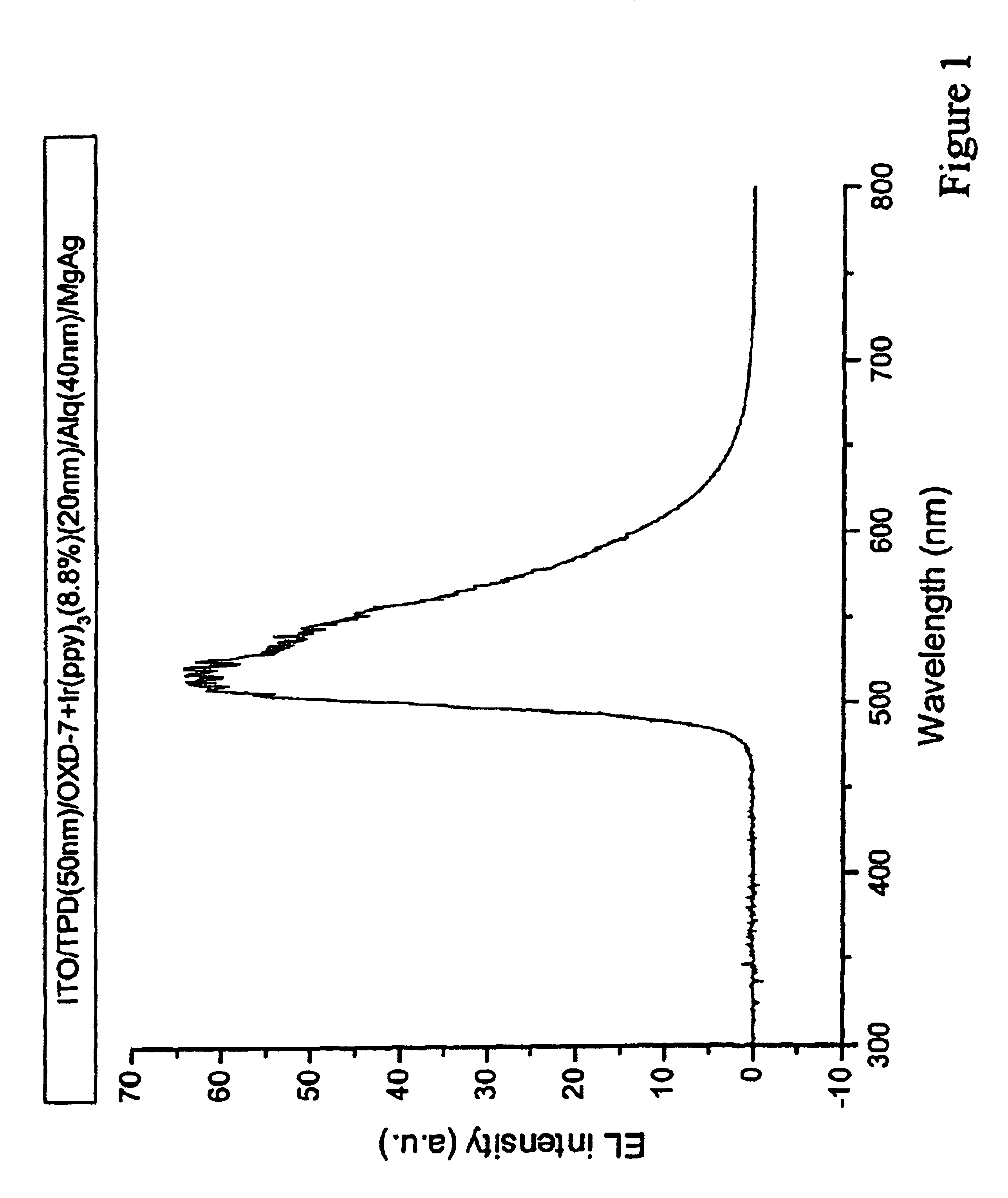
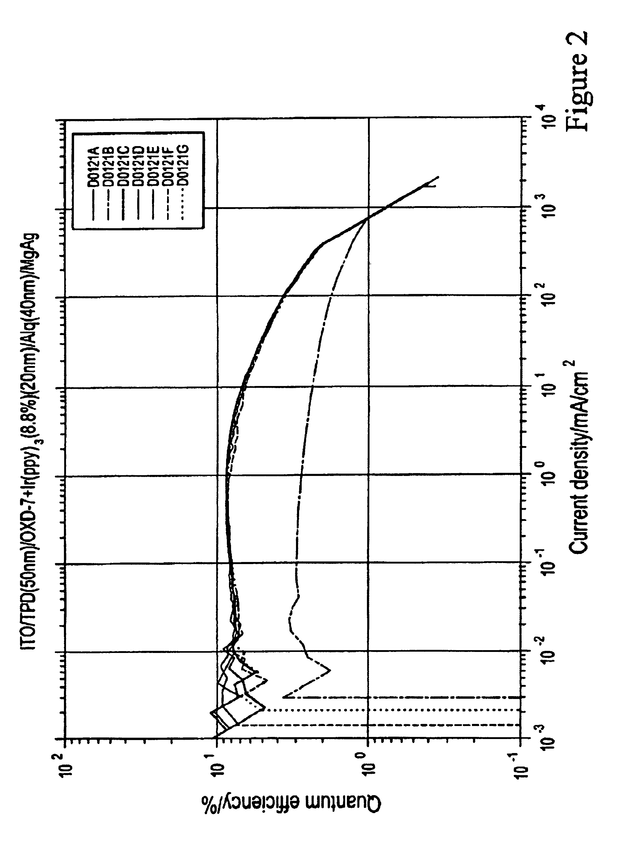
[0101]A hole transporting layer (“HTL”) is first deposited onto the ITO (indium tin oxide) coated glass substrate. The HTL consists of 30 nm (300 Å) of NPD. A first electron transporting layer, which is also a blocking layer, consisting of TAZ, having a thickness of about 20 nm (200 Å) is deposited onto the HTL layer. The first electron transporting layer is doped with Ir(ppy)3. A second electron transport layer of Alq3 having a thickness of about 20 nm is deposited onto the first electron transporting layer. The device is finished by depositing a Mg—Ag electrode onto the second electron transporting layer. This Mg-Ag electrode has of thickness 100 nm. All of the depositions are carried out at a vacuum less than 5×10⁻⁵ Torr. The devices are tested in air, without packaging.

[0102]When a voltage is applied between the cathode and the anode, holes are injected from ITO to NPD and transported by the NPD layer, while electrons are injected from MgAg to Alq3 and transported through Alq3. ...

example 2

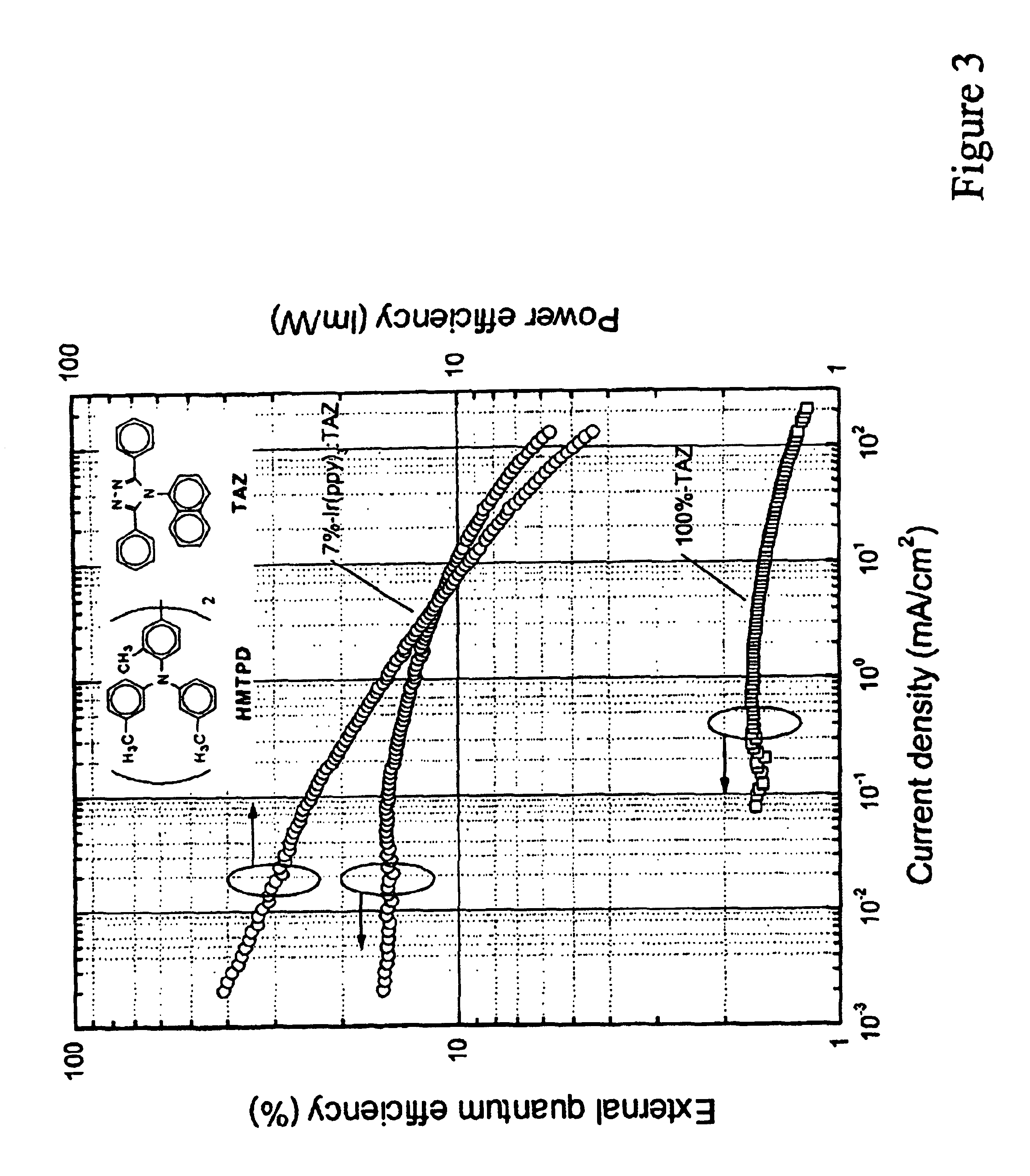
[0103]Organic layers were deposited by high vacuum (10−6 Torr) thermal evaporation onto a clean glass substrate precoated with an ITO layer. A 60 nm-thick film of 4,4′-bis[N,N′-(3-tolyl)amino]-3,3′-dimethylbiphenyl (HMTPD) serves as the HTL. Next a 25 nm-thick EML consisting of 6% to 8% Ir(ppy)3 is doped into various electron transporting hosts via thermal co-deposition. A 50 nm-thick layer of the electron transport material tris-(8-hydroxyquinoline) aluminum (Alq3) is used to transport and inject electrons into the EML. A shadow mask with 1 mm-diameter openings was used to define the cathode consisting of a 150 nm-thick magnesium silver (Mg—Ag) layer, with a 20 nm-thick Ag cap. Alternatively, the cathode consisted of a 100 nm-thick layer of aluminum-0.56wt % lithium.

[0104]Current density (J) versus voltage (V) measurements were obtained using a semiconductor parameter analyzer, with the luminance (L) obtained by placing the OLEDs directly onto the surface of a calibrated silicon ph...


PUM

PropertyMeasurementUnit
transparencyaaaaaaaaaa
energyaaaaaaaaaa

Abstract

An organic light emitting device structure having an organic light emitting device (OLED) over a substrate, where the OLED has, for example, an anode, a hole transporting layer (HTL), a first electron transporting layer (ETL) that is doped with a phosphorescent material, a second electron transporting layer (ETL), and a cathode. The OLEDs of the present invention are directed, in particular, to devices that include an emissive layer comprised of an electron transporting host material having a triplet excited state energy level that is higher than the emissive triplet excited state energy level of the phosphorescent dopant material.

Description

[0001]The present application claims the benefit under 35 U.S.C. 119(e) of provisional application 60 / 207,330, filed May 30, 2000.GOVERNMENT RIGHTS[0002]This invention was made with Government support under Contract No. F33615-94-1-1414 awarded by DARPA. The government has certain rights in this invention.FIELD OF THE INVENTIONResearch Agreements[0003]The claimed invention was made by, on behalf of, and / or in connection with one or more of the following parties to a joint university-corporation research agreement: Princeton University, The University of Southern California, and Universal Display Corporation. The agreement was in effect on and before the date the claimed invention was made, and the claimed invention was made as a result of activities undertaken within the scope of the agreement.<?insert-end id="INS-S-00001" ?>[0004]The present invention provides high efficiency phosphorescent organic light emitting devices. The present invention relates, for example, to an orga...

Claims


Application Information

Patent Timeline
Patent Type & Authority Patents(United States)
IPC IPC(8): H05B33/14H01L51/54H01L51/00H01L51/30H01L51/50
CPCY10S428/917H10K85/60H10K85/656H10K85/6572H10K85/341H10K50/11H10K2101/40H10K2101/10H10K50/14
Inventor ADACHI, CHIHAYABALDO, MARC A.FORREST, STEPHEN R.
Owner UNIV OF SOUTHERN CALIFORNIA
Why Eureka
Try Eureka