Imaging apparatus with two image sensors
a technology of image sensor and image, applied in the field of image sensor, can solve problems such as the generation of unnatural portions in images, and achieve the effect of high-quality recording and accurate focus detection
- Summary
- Abstract
- Description
- Claims
- Application Information
AI Technical Summary
Benefits of technology
Problems solved by technology
Method used
Image
Examples
first exemplary embodiment
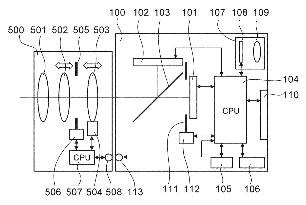
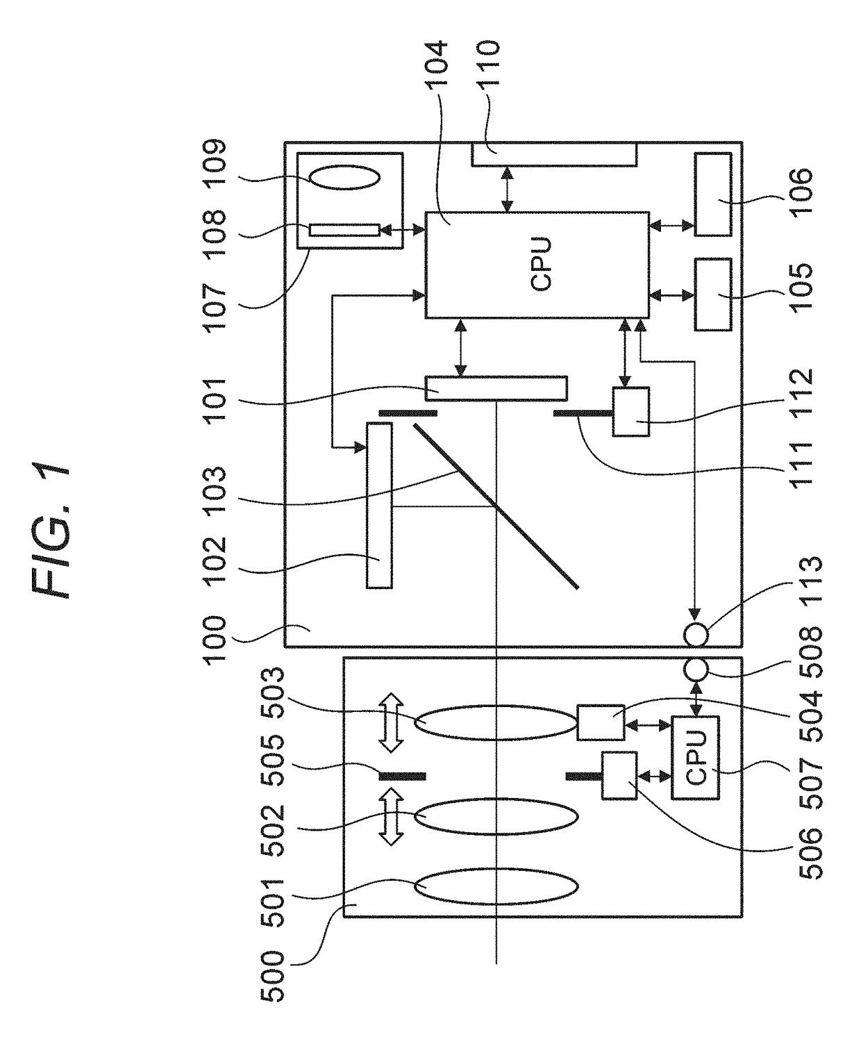
[0032]FIG. 1 is a configuration diagram of an interchangeable-lens digital camera main body 100 and an imaging lens 500 being an interchangeable lens, which serve as an example of an imaging apparatus to which the disclosure is applied.
[0033]A light beam transmitted through lens groups 501 to 503 of the imaging lens 500 enters a beam splitter 103 serving as a light beam splitter, or splitting unit, that is provided in the camera main body 100. The beam splitter 103 is fixed in the camera main body 100, and is a half mirror in the present exemplary embodiment. One light beam of light beams split by the beam splitter 103 is transmitted through the beam splitter 103 to be guided to an image sensor 101 serving as a first image sensor that is disposed on a first imaging plane. The other light beam is reflected on the beam splitter 103 to be guided to an image sensor 102 serving as a second image sensor that is disposed on a second imaging plane. In addition, the beam splitter 103 may not...
second exemplary embodiment
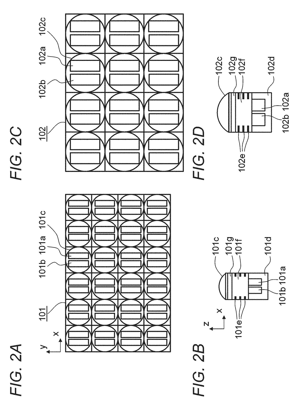
[0171]In the first exemplary embodiment, as illustrated in FIGS. 4A and 4B, by making the pixel size in the image sensor 101 for still images smaller than that in an image sensor for movies, and also shifting the focus position of the micro lens with respect to the photoelectric conversion units, the overlap between the pupil regions in the image sensor 101 for still images is made larger. In the second exemplary embodiment described below, characteristics similar to those in the first exemplary embodiment are obtained by providing a waveguide in a pixel portion of one image sensor. The shapes on the imaging plane of an image sensor 201 serving as a first image sensor and an image sensor 202 serving as a second image sensor according to the second exemplary embodiment are the same as those of the image sensors 101 and 102 illustrated in FIGS. 2A to 2D. In addition, the readout circuit configurations of the image sensors 201 and 202 are the same as that illustrated in FIG. 3. In addi...
third exemplary embodiment
[0182]In the following third exemplary embodiment, by employing a so-called rear surface irradiation type CMOS image sensor as one image sensor, and employing a front surface irradiation type CMOS image sensor as the other image sensor similarly to the above-described exemplary embodiments, the characteristics similar to those in the first and second exemplary embodiments are obtained. The shapes on the imaging plane of an image sensor 301 serving as a first image sensor and an image sensor 302 serving as a second image sensor according to the third exemplary embodiment are the same as those illustrated in FIGS. 2A to 2D. In addition, the readout circuit configuration of each image sensor is the same as that illustrated in FIG. 3. In addition, the structure of the image sensor 302 according to the third exemplary embodiment is the same as the structure of the image sensor 102 according to the first exemplary embodiment. Thus, the description of the parts having the same configuratio...
PUM
 Abstract
Description
Claims
Application Information
 - R&D
- Intellectual Property
- Life Sciences
- Materials
- Tech Scout
- Unparalleled Data Quality
- Higher Quality Content
- 60% Fewer Hallucinations
Browse by: Latest US Patents, China's latest patents, Technical Efficacy Thesaurus, Application Domain, Technology Topic, Popular Technical Reports.
© 2025 PatSnap. All rights reserved.Legal|Privacy policy|Modern Slavery Act Transparency Statement|Sitemap|About US| Contact US: help@patsnap.com


