Magnetic detection device
- Summary
- Abstract
- Description
- Claims
- Application Information
AI Technical Summary
Benefits of technology
Problems solved by technology
Method used
Image
Examples
examples
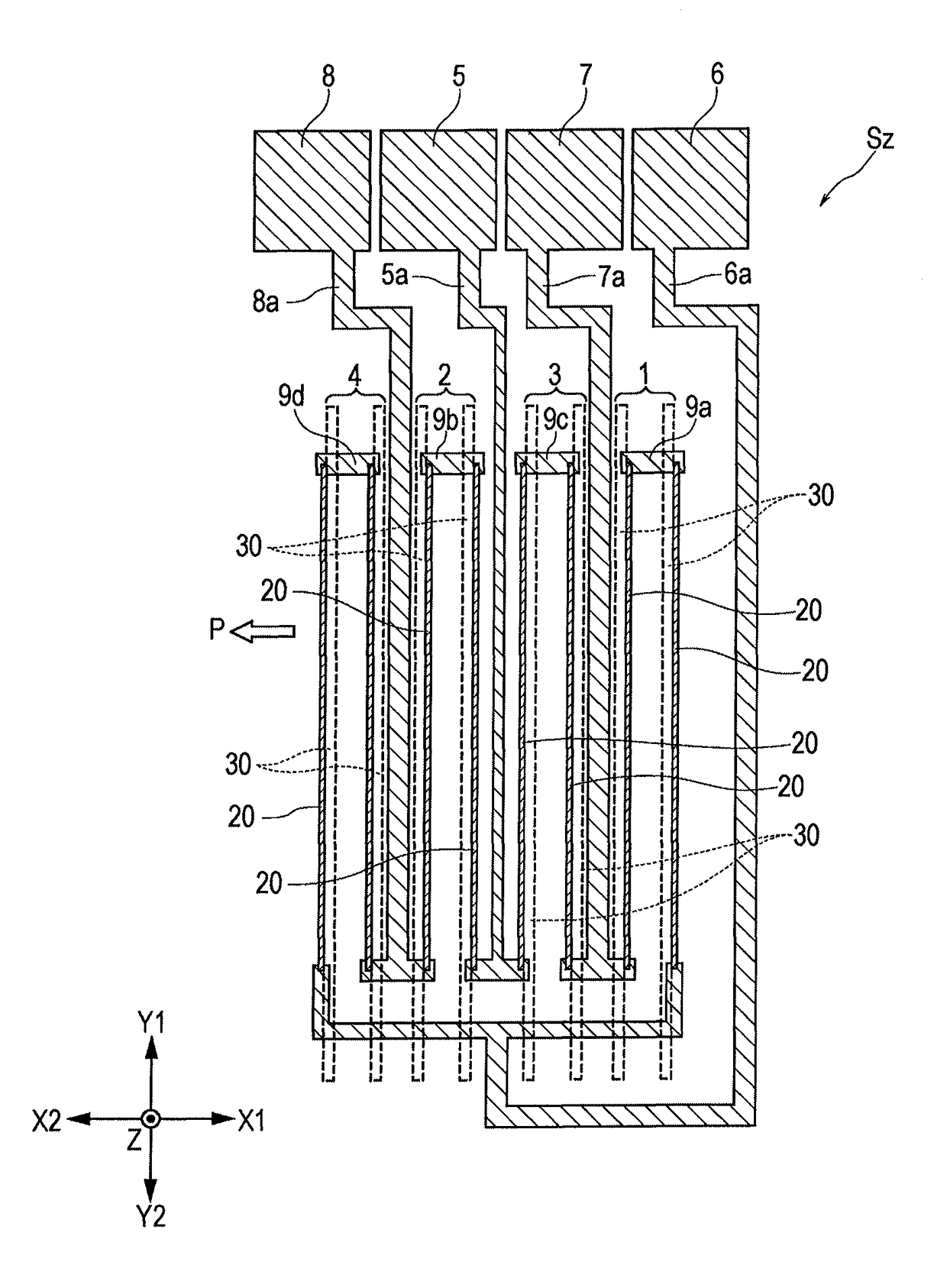
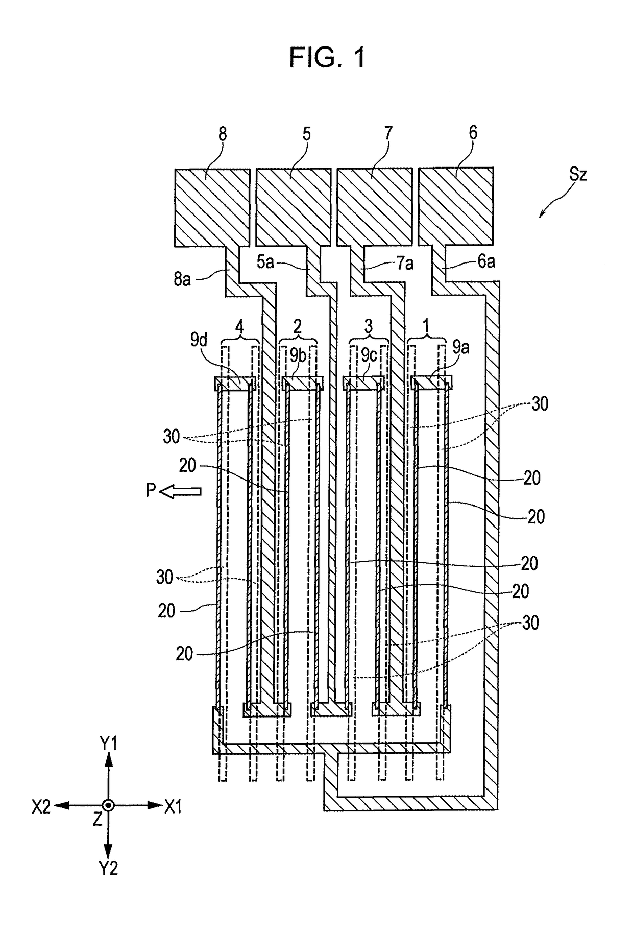
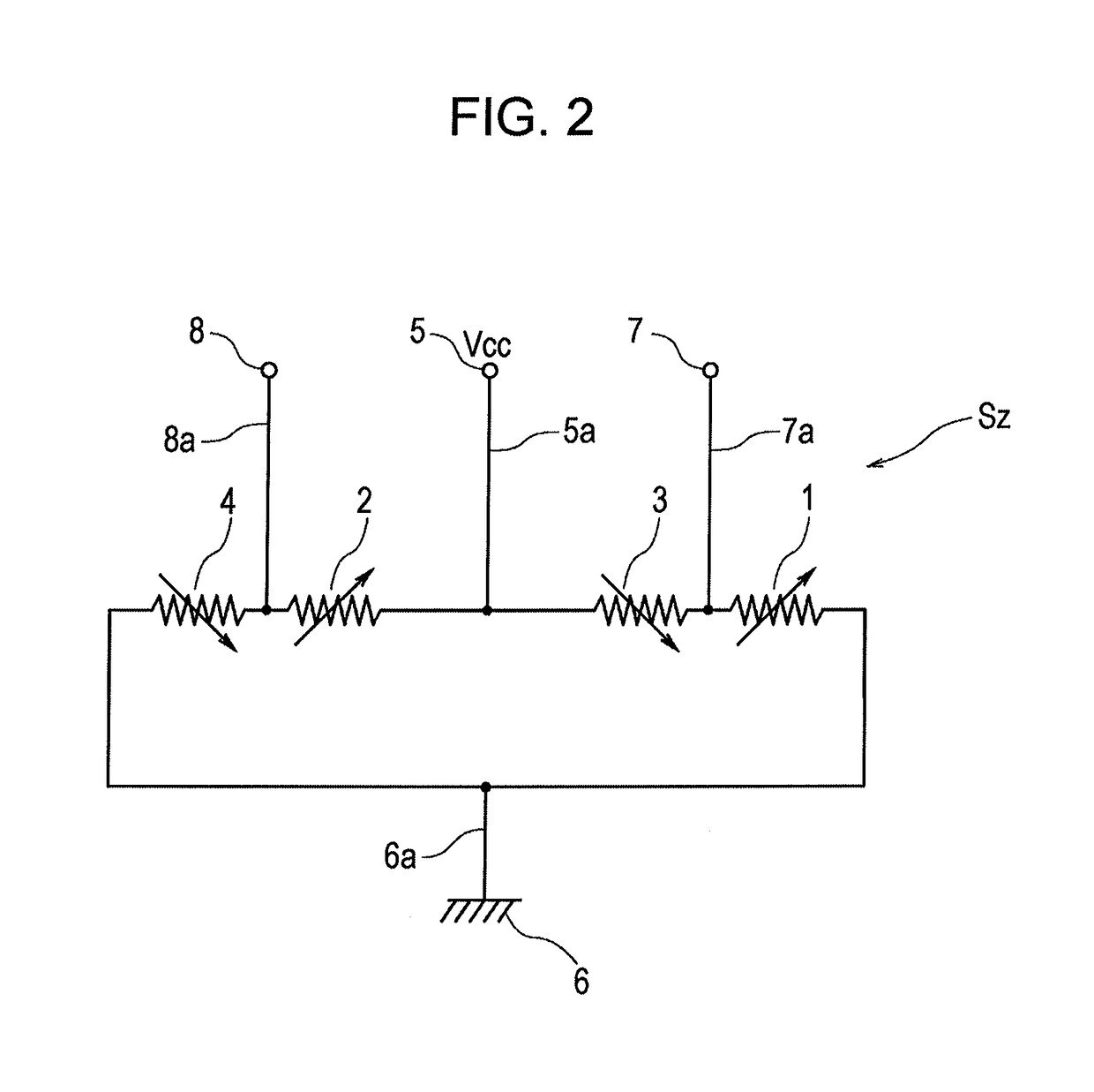
[0062]Table 1 and FIGS. 9 to 11 show sample numbers 1 to 9. A plurality of magnetic detection devices Sz were formed on a single wafer together. The sample numbers 1 to 9 are wafer numbers, and a plurality of magnetic detection devices Sz of the same sample number were formed for each sample number. In an example, a detection sensitivity and an offset of a detection output were measured using each magnetic detection device Sz. The width dimension of each magnetic sensor 20 in the X direction was set to 2 μm, and the length dimension of each magnetic sensor 20 in the Y direction was set to 150 mm. The height dimension of each magnetic field guide layer 30 in the Z direction was set to 95 μm, and the width dimension of each magnetic field guide layer 30 in the X direction was set to 5 μm.
[0063]As shown in Table 1, the configurations of the magnetic field guide layers 30 of the respective samples 1 to 9 are different from each other. In Table 1, “Bot” indicates the height dimension of ...
PUM
 Abstract
Description
Claims
Application Information
 - R&D
- Intellectual Property
- Life Sciences
- Materials
- Tech Scout
- Unparalleled Data Quality
- Higher Quality Content
- 60% Fewer Hallucinations
Browse by: Latest US Patents, China's latest patents, Technical Efficacy Thesaurus, Application Domain, Technology Topic, Popular Technical Reports.
© 2025 PatSnap. All rights reserved.Legal|Privacy policy|Modern Slavery Act Transparency Statement|Sitemap|About US| Contact US: help@patsnap.com


