Spread spectrum clock generator, electronic apparatus, and spread spectrum clock generation method
a technology of spread spectrum clock and generator, applied in the direction of single pulse train generator, pulse automatic control, pulse technique, etc., can solve the problem of generating phase error between the reference clock of the pll
- Summary
- Abstract
- Description
- Claims
- Application Information
AI Technical Summary
Benefits of technology
Problems solved by technology
Method used
Image
Examples
embodiment 1
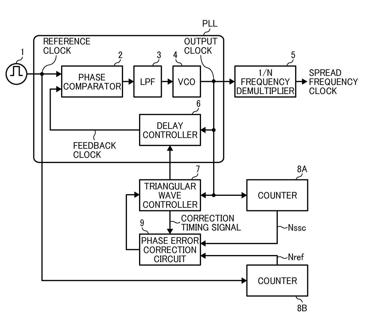
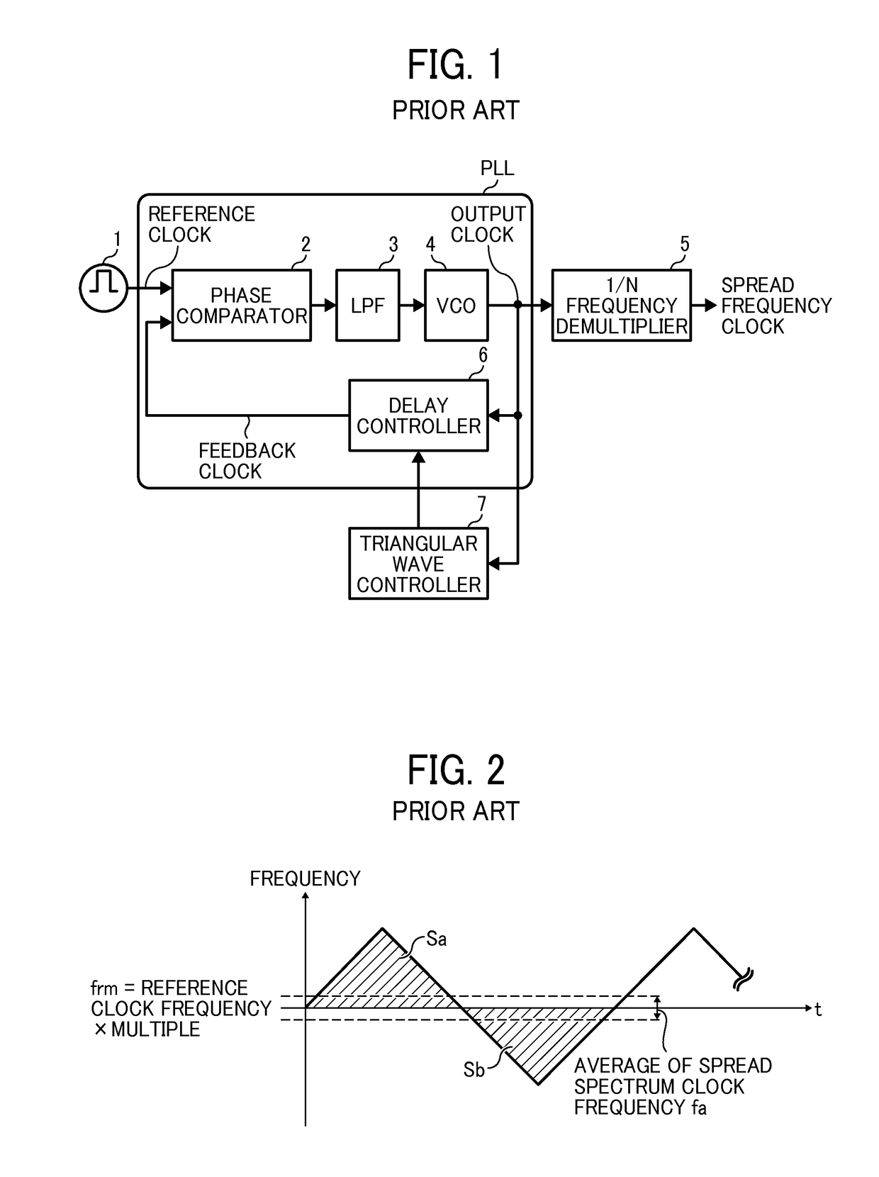
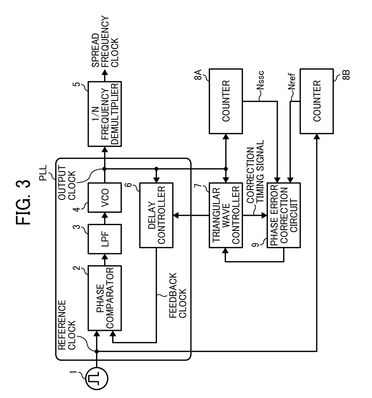
[0024]Furthermore, in the spread spectrum clock generator using the center spread method that multiplies the reference clock by a multiple, it is preferable that the average frequency of the spread spectrum clock matches the reference frequency frm indicated by x-axis in FIG. 2. However, actually, due to analog characteristics of the LPF 3 and circuit characteristics of the delay controller 6 in FIG. 1, even if the ideal triangular wave signal is used for delay control of the spread spectrum clock, usually the result is above the x-axis or below the x-axis. Here, in the ideal triangular wave signal, the area Sa on the plus-side of the reference frequency frm of the spread spectrum clock in FIG. 2 is the same as the area Sb on the minus-side of the reference frequency frm (i.e., their absolute integrated values are the same). In this case, if an ideal average frequency is achieved using the LPF 3 as an analog circuit with an attached analog circuit or the delay control circuit, typic...
embodiment 2
[0043]As described above, in this embodiment, the phase error correction circuit 9 compares the count value Nssc with the count value Nref for each frequency modulation period. Subsequently, in accordance with the comparison result, the phase error correction circuit 9 performs the phase error correction process so that the count value Nref gets close to the count value Nssc (i.e., the frequency of the output clock fssc gets close to the frequency of the reference clock fref substantially). As a result, in the spread spectrum clock generator using the PLL, it is possible to minimize the phase error, and it is possible that the frequency of the spread spectrum clock gets close to the frequency of the reference clock substantially. Embodiment 2 FIG. 5 is a diagram illustrating a waveform of the digital triangular wave signal for frequency modulation to explain a phase error correction process performed by a phase error correction circuit 9 in this embodiment. The delay controller 6 in...
embodiment 3
[0048]In this embodiment, in the operation (B), if Nssc is larger than Nref, in the subsequent frequency modulation period, the phase error correction circuit 9 generates the triangular wave signal whose minimum value period Nb is (n+1)Tc. It should be noted that the case described above is an example, and it is possible that the phase error correction circuit 9 generates the triangular wave signal whose maximum value period Nu is (n−1)Tc. Embodiment 3 FIG. 6 is a diagram illustrating a waveform of the digital triangular wave signal for frequency modulation to explain a phase error correction process performed by the phase error correction circuit 9 in this embodiment. In the embodiments 1 and 2, the phase error correction process is performed for each period of the frequency modulation period. However, in this embodiment, the phase error correction circuit 9 performs the phase error correction process for each period that the frequency modulation period is multiplied by a multiple ...
PUM
 Abstract
Description
Claims
Application Information
 - R&D
- Intellectual Property
- Life Sciences
- Materials
- Tech Scout
- Unparalleled Data Quality
- Higher Quality Content
- 60% Fewer Hallucinations
Browse by: Latest US Patents, China's latest patents, Technical Efficacy Thesaurus, Application Domain, Technology Topic, Popular Technical Reports.
© 2025 PatSnap. All rights reserved.Legal|Privacy policy|Modern Slavery Act Transparency Statement|Sitemap|About US| Contact US: help@patsnap.com


