
Liquid crystal display device

a liquid crystal display and liquid crystal technology, applied in non-linear optics, instruments, optics, etc., can solve the problems of liquid crystal molecules being more likely to rise and blur on the screen, and achieve the effect of increasing screen luminance and reducing disclination area

Inactive Publication Date: 2017-10-31
JAPAN DISPLAY INC
View PDF11 Cites 0 Cited by
  • Summary
  • Abstract
  • Description
  • Claims
  • Application Information

AI Technical Summary

Benefits of technology

[0010]All of the LCD devices mentioned in the background section use liquid crystals with positive dielectric anisotropy (hereinafter referred to simply as ‘positively anisotropic LCs’). Positively anisotropic LCs are ones in which the long axes of their molecules face the direction of electric fields. On the other hand, liquid crystals with negative dielectric anisotropy (hereinafter referred to simply as ‘negatively anisotropic LCs’) are ones in which the short axes of their molecules face the direction of electric fields. Positively anisotropic LCs are prone to the problem of disclination stated above. When disclination occurs within a certain area of a pixel, light is not transmitted at that area, resulting in reduced transmittance of the pixel and reduced luminance of the screen.
[0014]Thus, an object of the present invention is to increase the luminance of an LCD and prevent the occurrence of blurs on the screen by suppressing disclination and preventing the liquid crystal molecules from rising in a direction normal to the TFT substrate when the screen is pressed.
[0015]The present invention is designed to address the above problems, and its main feature is that it adopts the use of negatively anisotropic LCs to suppress the occurrence of disclination and to prevent the liquid crystal molecules from rising in a direction normal to the TFT substrate when the screen is pressed. In negatively anisotropic LCs, polar groups are located on the short-axis side of the liquid crystal molecules. Thus, in terms of molecular structure, negatively anisotropic LCs have a smaller dielectric anisotropy Δ∈ than positively anisotropic LCs. Also, in the case of negatively anisotropic LCs, the rotation of liquid crystal molecules due to voltage application is less likely to occur than in the case of positively anisotropic LCs.
[0016]In the present invention, negatively anisotropic LCs are used with the particular intentions stated above, and by adopting the pixel electrode shape that suits the negatively anisotropic LCs, their excellent characteristics can be exploited. As a result, the luminance of the screen can be improved, and the screen is less likely to have a blur when pressed. The following are the specific means for achieving the above object.
[0022]The present invention allows an IPS LCD to have a reduced area of disclination and increased screen luminance. Moreover, because the liquid crystal molecules become less likely to rise in a direction normal to the TFT substrate, the screen is less likely to have an image blur when pressed.

Problems solved by technology

Positively anisotropic LCs are prone to the problem of disclination stated above.
Another problem of positively anisotropic LCs is that the liquid crystal molecules are more likely to rise in a direction normal to the TFT substrate when the screen is pressed (see FIG. 4A).
Also, in the case of an IPS LCD, such rising of LC molecules often leads to a blur on the screen.

Method used


Image

  • Liquid crystal display device
  • Liquid crystal display device
  • Liquid crystal display device

Examples


embodiment 1

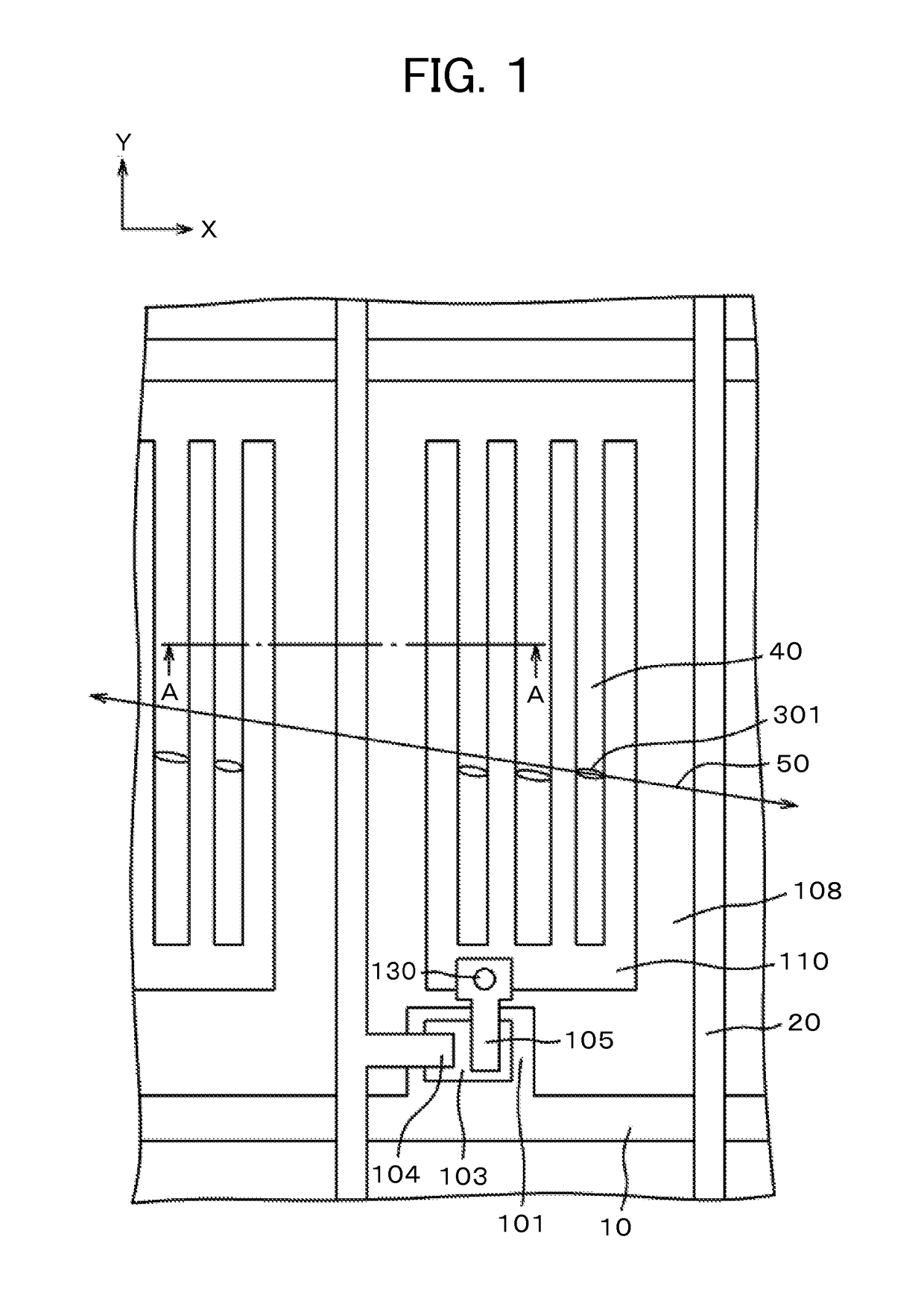
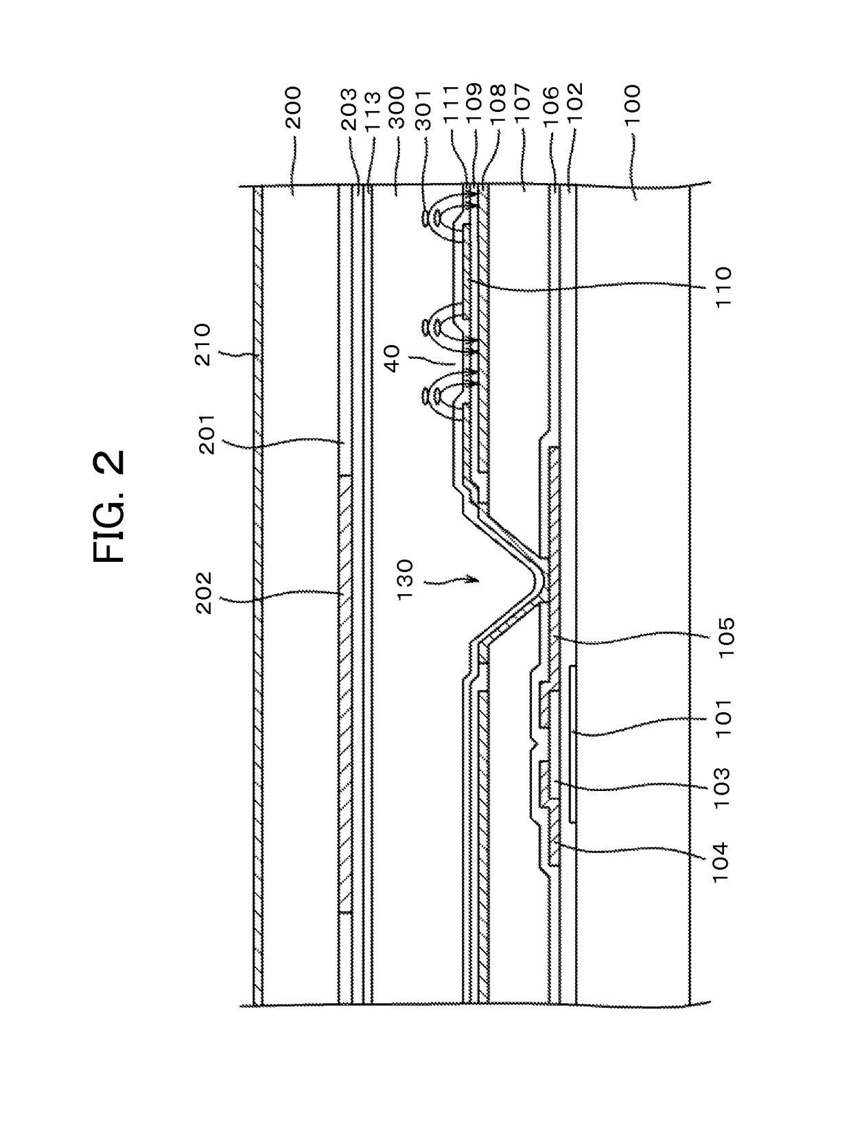
[0034]FIG. 1 is a plan view illustrating the structure of a pixel according to Embodiment 1 of the present invention while FIG. 2 is a cross section of the pixel. FIG. 3 is a cross section taken along line A-A of FIG. 1. In the present invention, negatively anisotropic LCs are used as liquid crystals 301. First, the pixel structure is described with reference to the cross section of FIG. 2. As illustrated in FIG. 2, a gate electrode 101 is formed on a glass-made TFT substrate 100, and a gate insulting film 102 is deposited on the gate electrode 101 and the TFT substrate 100. A semiconductor layer 103 is formed above the gate electrode 101 with the gate insulating film 102 located therebetween.

[0035]The semiconductor layer 103 is formed of a-Si. For electrical connection with a drain electrode 104 and a source electrode 105, the semiconductor layer 103 also includes n+a-Si. An inorganic passivation film 106 is deposited on the semiconductor layer 103, drain electrode 104, and source ...

embodiment 2

[0059]An IPS LCD has excellent viewing angle characteristics, but they may vary depending on the directions in which the viewer sees the screen, that is, on azimuth angles. To counter this, there is a method called the quasi-dual-domain scheme. In the method, two types of pixels in which the liquid crystal molecules rotate in different directions are used, and the azimuth angle characteristics are made uniform by particular combinations of these two types of pixels.

[0060]FIG. 8 is a plan view of a pixel of a quasi-dual-domain LCD according to Embodiment 2 of the invention. In FIG. 8, the alignment axis 50 extends in the x direction. The long axis of the slits 40 of a pixel electrode 110 is tilted by +θ degrees with respect to a direction perpendicular to the alignment axis 50. In this case, application of a voltage to the pixel electrode 110 causes the liquid crystal molecule to rotate in the left direction.

[0061]Though not illustrated, the pixel electrodes of the two pixels located...

embodiment 3

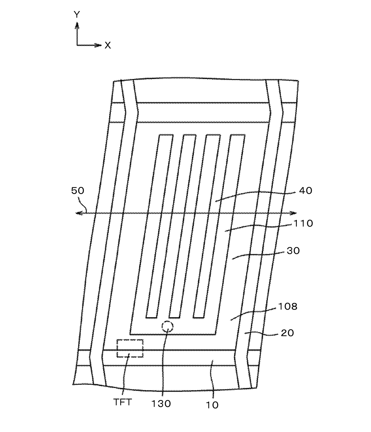
[0063]In another method for lessening the dependency of viewing angle characteristics on azimuth angles, two domains in which liquid crystal molecules rotate in different directions are created within a pixel. FIG. 9 is an example of a pixel of such an LCD to which the invention is applied. As illustrated in FIG. 9, two data lines 20 that outline the pixel are bent near the center of the pixel, and a pixel electrode 110 includes upper and lower slits 40 that extend from its central bus electrode. The alignment axis 50 of the alignment film extends in the x direction. Although the upper half and lower half of the pixel electrode 110 are both in the shape of a comb, the long-axis angle of the teeth of the upper half with respect to a direction perpendicular to the alignment axis 50 (i.e., with respect to the y-axis) is opposite to that of the lower half. In other words, the upper and lower slits 40 of the pixel electrode 110 have different long-axis angles with respect to the y-axis.

[...


PUM

PropertyMeasurementUnit
thicknessaaaaaaaaaa
transmittance rateaaaaaaaaaa

Abstract

An IPS LCD that not only increases the screen luminance but also prevents the occurrence of image blurs by reducing the area of disclination and preventing the liquid crystal molecules from rising in a direction normal to the TFT substrate. A pixel electrode is disposed in the pixel surrounded by two gate lines and two data lines. A planar common electrode is located below the pixel electrode with an inter-layer insulating film provided therebetween. The pixel electrode includes slits each being open at the edge on one side and has the shape of a comb. Liquid crystals with negative dielectric anisotropy are used as liquid crystal. The above structure increases the transmissive area of the pixel up to the open edges of the slits and also prevents the liquid crystal molecules from rising in a direction normal to the TFT substrate, thereby preventing the occurrence of blurs.

Description

CLAIM OF PRIORITY[0001]The present application claims priority from Japanese Patent Application JP 2014-006748 filed on Jan. 17, 2014, the content of which is hereby incorporated by reference into this application.BACKGROUND OF THE INVENTION[0002]1. Field of the Invention[0003]The present invention relates to display devices and particularly to an IPS liquid crystal display with excellent viewing angle characteristics and increased luminance.[0004]2. Description of the Related Art[0005]A typical liquid crystal display (LCD) includes a TFT substrate, a counter substrate, and a liquid crystal layer. On the TFT substrate, pixels each having a pixel electrode, a thin film transistor (TFT), and the like are formed in the form of a matrix. The counter substrate is disposed so as to face the TFT substrate with the liquid crystal layer sandwiched therebetween. On the surface of the counter substrate that faces the TFT substrate, color filters are formed such that they are located above the ...

Claims


Application Information

Patent Timeline
Patent Type & Authority Patents(United States)
IPC IPC(8): G02F1/1343G02F1/1337
CPCG02F1/134309G02F1/134363G02F1/133707
Inventor TSURUMA, TAKEYUKIYAMAGUCHI, HIDEMASA
Owner JAPAN DISPLAY INC
Learn More