Thin-film photoelectric converter

a photoelectric converter and thin film technology, applied in the field of thin film photoelectric converters, can solve the problems of significantly thereby reducing power generation efficiency, so as to prevent deterioration in long-term use, reduce the diffusivity of impurities such as oxygen, and reduce the photoelectric conversion efficiency

Inactive Publication Date: 2017-07-18
MITSUBISHI ELECTRIC CORP
View PDF28 Cites 2 Cited by
  • Summary
  • Abstract
  • Description
  • Claims
  • Application Information

AI Technical Summary

Benefits of technology

[0015]In the thin-film photoelectric converter utilizing a microcrystalline film serving as a photoelectric conversion layer according to the present invention, all the side wall portions of the photoelectric conversion layer are surrounded by amorphous films which are less to be oxidized than the microcrystalline film and in which the diffusivity of impurities such as oxygen is low. This can prevent the ingress of impurities such as oxygen into the photoelectric conversion layer due to oxidation. Therefore, a reduction in the photoelectric conversion efficiency due to the ingress of impurities into the photoelectric conversion layer is prevented, and deterioration in long-term use is thereby prevented. This provides an advantageous effect in that the long-term reliability of the thin-film photoelectric converter can be improved.

Problems solved by technology

Impurities present in the silicon film also reduce the power generation efficiency.
In particular, when the thin-film semiconductor layer is a microcrystalline silicon film, the oxidation of the microcrystalline silicon film due to the ingress of oxygen into the silicon film significantly reduces the power generation efficiency.
However, when the crystals are mainly oriented in (111), the ingress of impurities is facilitated, and the power generation efficiency is thereby reduced.

Method used


Image

  • Thin-film photoelectric converter
  • Thin-film photoelectric converter
  • Thin-film photoelectric converter

Examples


first embodiment

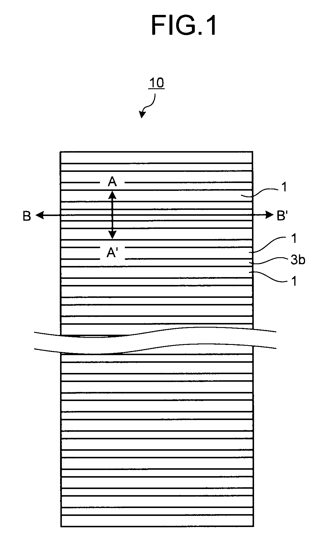
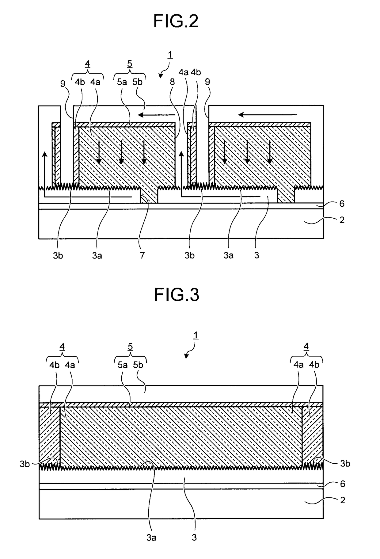
[0049]FIG. 1 is a plan view illustrating the schematic structure of a thin-film photoelectric conversion module (hereinafter referred to as a module) 10, which is a thin-film photoelectric converter according to a first embodiment of the present invention. FIG. 2 is a cross-sectional view of a principal part taken along line segment A-A′ in FIG. 1, illustrating the cross-sectional structure of the module 10. FIG. 3 is a cross-sectional view taken along line segment B-B′ in FIG. 1, illustrating the longitudinal cross-sectional structure of a unit thin-film photoelectric conversion cell (which hereinafter may be referred to as a unit cell) 1 constituting the module 10.

[0050]As illustrated in FIGS. 1 to 3, the module 10 according to the first embodiment includes a plurality of strip-shaped (rectangular) unit cells 1 and has a structure in which these unit cells 1 are connected in series. Each of the unit cells 1 has a structure in which a transparent electrode layer 3 serving as a firs...

second embodiment

[0079]FIG. 6 is a plan view illustrating the schematic structure of a thin-film photoelectric conversion module (hereinafter referred to as a module) 20 of a thin-film photoelectric converter according to a second embodiment of the present invention. FIG. 7 is a cross-sectional view of a principal part taken along line segment C-C′ in FIG. 6, illustrating the cross-sectional structure of the module 20. FIG. 8 is a cross-sectional view taken along line segment D-D′ in FIG. 6, illustrating the longitudinal cross-sectional structure of a unit cell 21 constituting the module 20. In the following figures, the same components as those in FIGS. 1 to 3 are denoted by the same reference numerals.

[0080]As illustrated in FIGS. 6 to 8, the module 20 according to the second embodiment includes a plurality of strip-shaped (rectangular) unit cells 21 and has a structure in which these unit cells 21 are connected in series. The module 20 has the same structure as the module 10 of the first embodime...

third embodiment

[0091]FIG. 12 is a plan view illustrating the schematic structure of a thin-film photoelectric conversion module (hereinafter referred to as a module) 40 of a thin-film photoelectric converter according to a third embodiment of the present invention. FIG. 13 is a cross-sectional view taken along line segment E-E′ in FIG. 12, illustrating the longitudinal cross-sectional structure of a unit cell 41 constituting the module 40. FIG. 14 is a plan view illustrating an insulating light-transmitting substrate 42 used in the module 40 according to the third embodiment. In the following figures, the same components as those in FIGS. 1 to 3 are denoted by the same reference numerals.

[0092]As illustrated in FIGS. 12 and 13, the module 40 according to the third embodiment includes a plurality of strip-shaped (rectangular) unit cells 41 and has a structure in which these unit cells 41 are connected in series. The module 40 has the same structure as the module 10 of the first embodiment except th...


PUM


Abstract

A thin-film photoelectric converter in which a first electrode layer formed of a transparent conductive material, a photoelectric conversion layer for photoelectric conversion, and a second electrode layer formed of a conductive material that reflects light are stacked in that order on an insulating light-transmitting substrate. The photoelectric conversion layer and the second electrode layer are divided by dividing grooves into islands that form a plurality of photoelectric conversion cells separated from each other, adjacent ones of the plurality of photoelectric conversion cells separated by the dividing grooves being electrically connected in series. The photoelectric conversion layer includes: a first semiconductor layer including a microcrystalline structure; and a second semiconductor layer including an amorphous structure, the second semiconductor layer being disposed so as to surround all side wall portions of the first semiconductor layer that extend in in-plane directions of the insulating light-transmitting substrate.

Description

TECHNICAL FIELD[0001]The present invention relates to a thin-film photoelectric converter and to a method for manufacturing the same.BACKGROUND ART[0002]In a conventional thin-film solar battery (thin-film photoelectric converter), thin-film solar battery cells (thin-film photoelectric conversion cells) are configured, for example, by forming a thin-film semiconductor layer serving as a photoelectric conversion layer on a substrate having a light-transmitting electrode formed thereon and forming a reflecting conductive film on a rear side. These solar battery cells generate photo-electromotive force when light is incident from the front side (light-transmitting electrode side).[0003]The thin-film solar battery is configured such that adjacent ones of a plurality of thin-film solar battery cells are spaced apart by a predetermined distance, and the thin-film solar battery cells are electrically connected in series. The photoelectric conversion layers between adjacent thin-film solar ...

Claims


Application Information

Patent Timeline
Patent Type & Authority Patents(United States)
IPC IPC(8): H01L31/0224H01L31/0236H01L31/18H01L31/0368H01L31/0392H01L31/046H01L31/0475H01L31/075H01L31/076
CPCH01L31/03921H01L31/02366H01L31/03685H01L31/046H01L31/1804H01L31/1824Y02E10/545Y02E10/547Y02E10/548Y02P70/521Y02P70/50
Inventor TOKIOKA, HIDETADAYAMARIN, HIROYA
Owner MITSUBISHI ELECTRIC CORP
Why Eureka
Try Eureka