Flexible electronic device having adhesive function and method of manufacturing the same
a flexible electronic device and function technology, applied in the direction of sustainable manufacturing/processing, transistors, final product manufacturing, etc., can solve the problems of increasing the number of manufacturing processes, device may still break, and not structurally compatible with existing two-dimensional planar devices, so as to achieve the effect of maintaining performance over a long period of time and minimizing the breakage of electronic devices
- Summary
- Abstract
- Description
- Claims
- Application Information
AI Technical Summary
Benefits of technology
Problems solved by technology
Method used
Image
Examples
example
Example 1
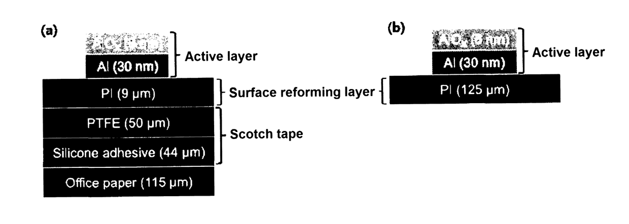
[0085]Scotch tape was prepared as the adhesive tape including polytetrafluoroethylene (PTFE) as the flexible film and the silicon-based adhesive as the adhesive layer (3M™, 5480, PTFE thickness of 50 μm, and silicon-based adhesive thickness of 44 μm). The Scotch tape was attached to the silicon wafer.
[0086]Next, the polyimide solution (VTEC™, P1-1388) was applied on the tape attached to the silicon wafer using spin coating at 3000 rpm for 30 sec, and sequentially baked at 60° C. and 150° C. for 10 min to form the polyimide surface reforming layer.
[0087]Next, the aluminum layer (30 nm), as the gate electrode, was deposited on the surface reforming layer using heat in the thermal deposition apparatus using the shadow mask.
[0088]The aluminum layer was then oxidized in the oxygen plasma chamber under the condition of RF power (radio frequency power) of 250 W for 7 min to form the gate insulating layer on the surface of the aluminum layer. Oxygen pressure was maintained as low a...
example 2
[0092]The graphene field-effect transistor was manufactured using the same method and condition as Example 1, except that the pressure of the oxygen plasma chamber was 50 mTorr rather than 12 mTorr when the gate insulating layer was formed.
example 3
[0093]The graphene field-effect transistor was manufactured using the same method and condition as Example 1, except that the pressure of the oxygen plasma chamber was 100 mTorr rather than 12 mTorr when the gate insulating layer was formed.
PUM
| Property | Measurement | Unit |
|---|---|---|
| root-mean-square roughness | aaaaa | aaaaa |
| thickness | aaaaa | aaaaa |
| RF power | aaaaa | aaaaa |
Abstract
Description
Claims
Application Information
 - R&D
- Intellectual Property
- Life Sciences
- Materials
- Tech Scout
- Unparalleled Data Quality
- Higher Quality Content
- 60% Fewer Hallucinations
Browse by: Latest US Patents, China's latest patents, Technical Efficacy Thesaurus, Application Domain, Technology Topic, Popular Technical Reports.
© 2025 PatSnap. All rights reserved.Legal|Privacy policy|Modern Slavery Act Transparency Statement|Sitemap|About US| Contact US: help@patsnap.com


