Display panel and display device
a display panel and display panel technology, applied in non-linear optics, instruments, optics, etc., can solve the problems of increasing design cost and compressed spacers in the sealant of the display panel, and achieve the effect of saving design cost and reducing design cos
- Summary
- Abstract
- Description
- Claims
- Application Information
AI Technical Summary
Benefits of technology
Problems solved by technology
Method used
Image
Examples
first embodiment
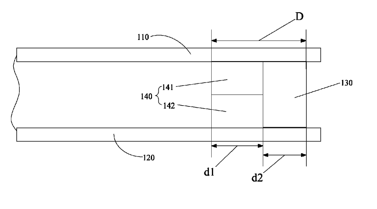
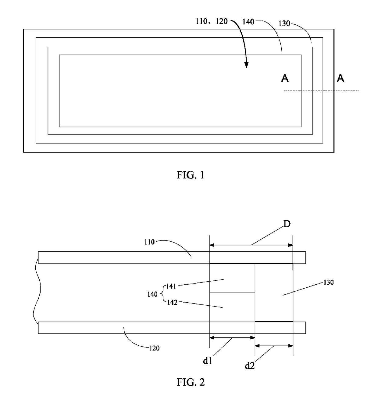
[0027]The present invention discloses a display device, and the display device includes a display panel. As shown in FIG. 1 and FIG. 2, FIG. 1 is schematic diagram of a display panel according to the present invention; FIG. 2 is a schematic diagram of a cross-sectional line A-A according to the display panel shown in FIG. 1.
[0028]The display panel includes a first substrate 110, a second substrate 120, a sealant 130, and at least one color resist layer 140. The first substrate 110 and the second substrate 120 are disposed separately. The sealant 130 is disposed surrounding and disposed between the first substrate 110 and the second substrate 120. The color resist layer 140 is disposed between the first substrate 110 and the second substrate 120. Wherein, the first substrate 110 is a thin-film-transistor array substrate, and the second substrate 120 is a color filter substrate. Or, the first substrate 110 is a color filter substrate, and the second substrate 120 is a thin-film-transi...
second embodiment
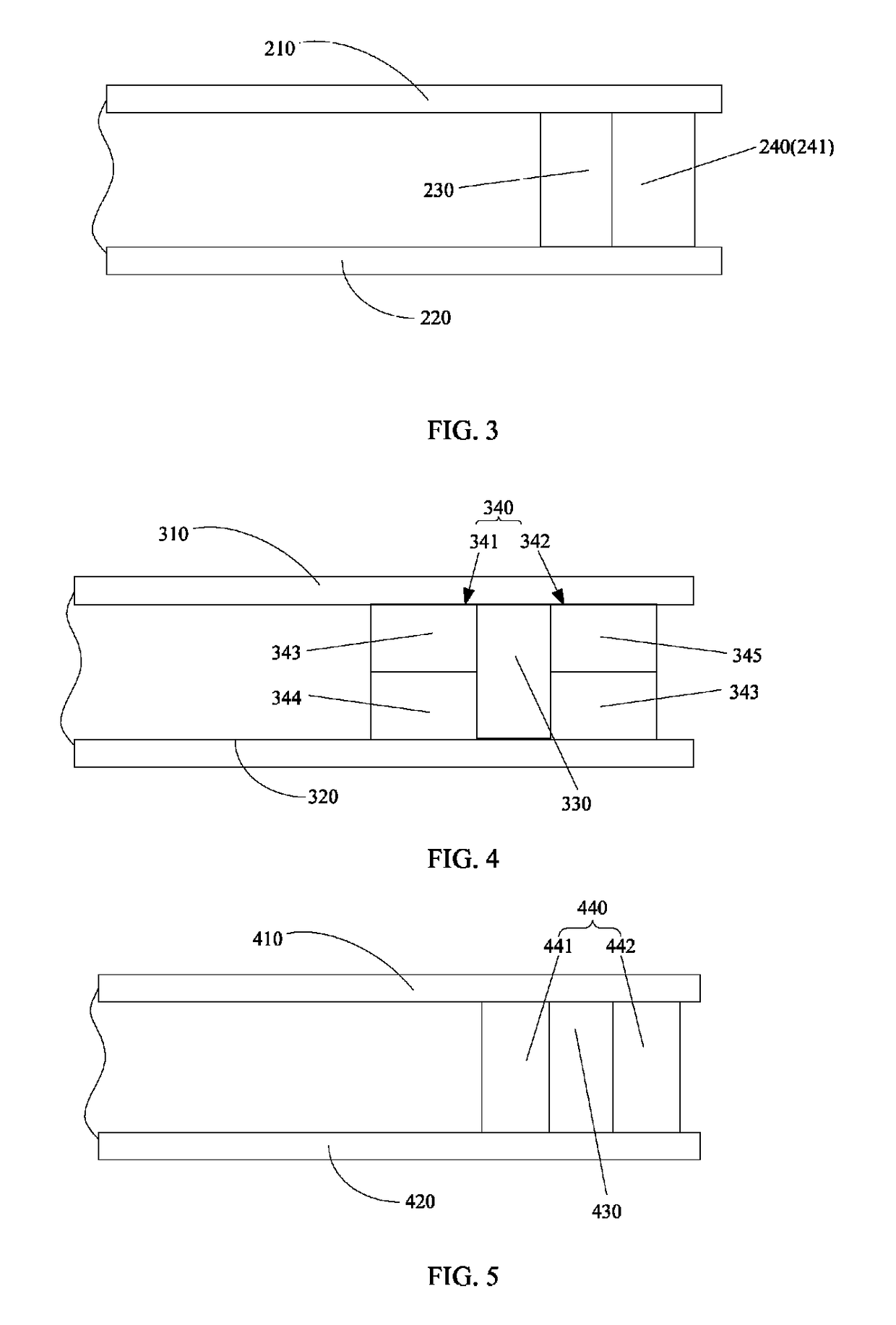
[0036]With reference to FIG. 3, FIG. 3 is a schematic diagram of a cross-sectional line A-A according to the display panel shown in FIG. 1. The first substrate 210 and the second substrate 220 in FIG. 3 correspond to the first substrate 110 and the second substrate 120 in FIG. 1. The main difference between the display panel in FIG. 3 and the display panel in FIG. 1 is: at least one color resist layer 240 is formed by one of a red sub-color resist 241, a green sub-color resist (not shown), and a blue sub-color resist (not shown) and is formed between the first substrate 210 and the second substrate 220 and is perpendicular to horizontal planes where the first substrate 210 and the second substrate 220 are disposed. In this embodiment, the at least one color resist layer 240 is formed by one layer of the red sub-color resist 241, and the red sub-color resist 241 is perpendicular to horizontal planes where the first substrate 210 and the second substrate 220 are located. Besides, the ...
third embodiment
[0038]With reference to FIG. 4, FIG. 4 is a schematic diagram of a cross-sectional line A-A according to the display panel shown in FIG. 1. The first substrate 310 and the second substrate 320 in FIG. 4 correspond to the first substrate 110 and the second substrate 120 in FIG. 1. The main difference between the display panel in FIG. 4 and the display panel in FIG. 1 is: at least one color resist layer 340 includes a first color resist layer 341 and a second color resist layer 342. The sealant 330 is disposed between the first color resist layer 341 and the second color resist layer 342. Wherein, the first color resist layer 341 and the second color resist layer 342 are respectively formed by at least two of a red sub-color resist 343, a green sub-color resist 344 and a blue sub-color resist 345 and is disposed between the first substrate 310 and the second substrate 320. The first color resist layer 341 and the second color resist layer 342 are in parallel with horizontal planes whe...
PUM
| Property | Measurement | Unit |
|---|---|---|
| width | aaaaa | aaaaa |
| width | aaaaa | aaaaa |
| thickness | aaaaa | aaaaa |
Abstract
Description
Claims
Application Information
 - R&D
- Intellectual Property
- Life Sciences
- Materials
- Tech Scout
- Unparalleled Data Quality
- Higher Quality Content
- 60% Fewer Hallucinations
Browse by: Latest US Patents, China's latest patents, Technical Efficacy Thesaurus, Application Domain, Technology Topic, Popular Technical Reports.
© 2025 PatSnap. All rights reserved.Legal|Privacy policy|Modern Slavery Act Transparency Statement|Sitemap|About US| Contact US: help@patsnap.com


