Imaging apparatus and imaging system
a technology of imaging system and imaging apparatus, which is applied in the direction of color television details, television system details, television systems, etc., can solve the problems of preventing the achievement of high-speed reading, and achieve the effect of suppressing the high-brightness darkening phenomenon without preventing the achievement of high-speed operation
- Summary
- Abstract
- Description
- Claims
- Application Information
AI Technical Summary
Benefits of technology
Problems solved by technology
Method used
Image
Examples
first embodiment
[0026](First Embodiment)
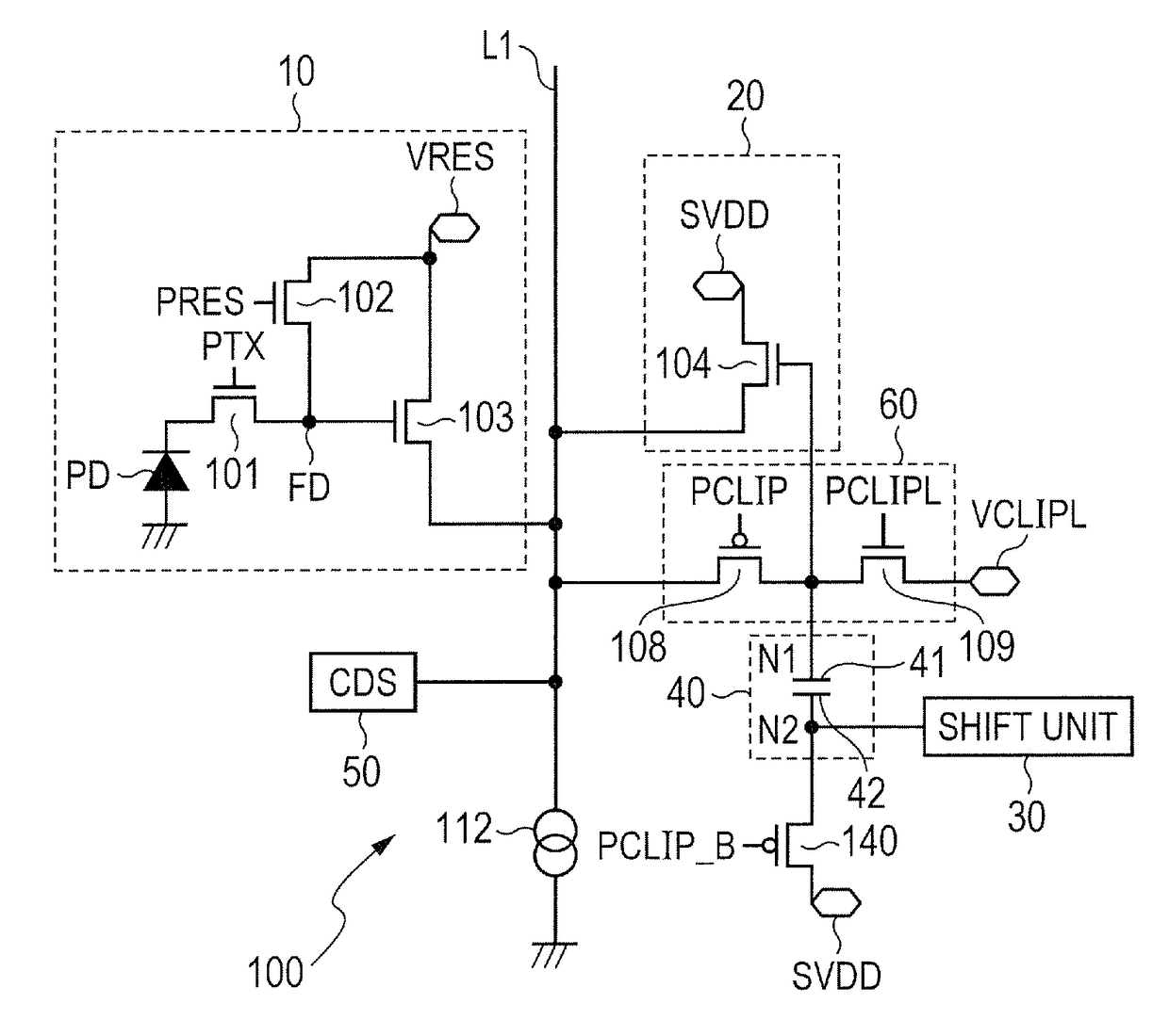
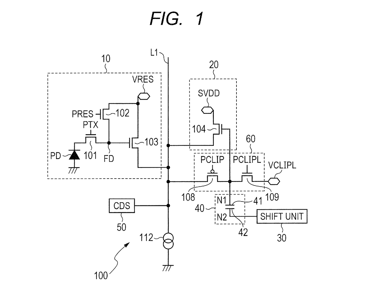
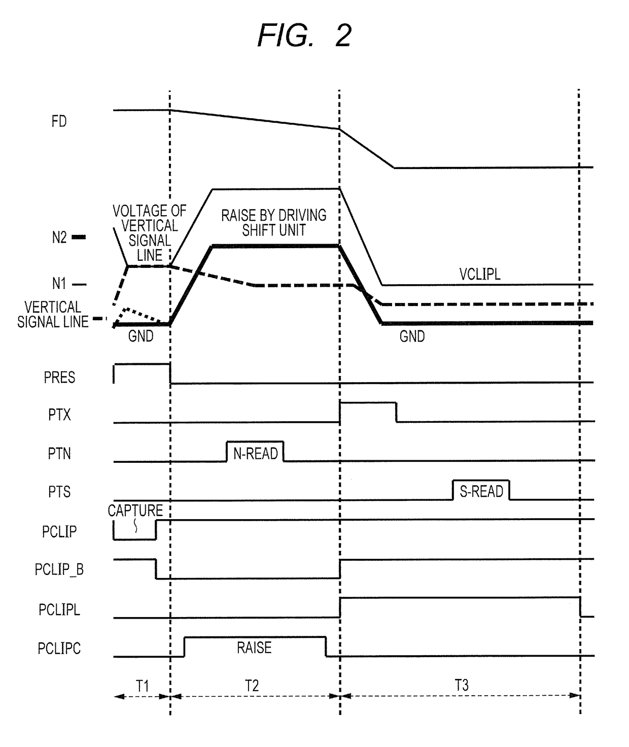
[0027]FIG. 1 is a circuit diagram illustrating a configuration example of an imaging apparatus 100 according to a first embodiment of the present invention. The imaging apparatus 100 includes pixels 10, switches 60, holding capacitors 40, a shift unit 30, clip units 20, and a CDS circuit (difference circuit) 50. The CDS circuit 50 is provided outside the imaging apparatus 100, and can externally perform a CDS process. The multiple pixels 10 are arranged in a two-dimensional matrix in an imaging area of the imaging apparatus 100. That is, the pixels 10 are arranged in a plurality of rows and a plurality of columns. The pixels 10 on the same column are connected to a vertical signal line L1. A plurality of vertical signal lines L1 is arranged corresponding to respective columns each on which the multiple pixels 10 are arranged. Each of the pixels 10 includes a photoelectric converting portion. PD, a transfer portion 101, a charge-to-voltage converting portion F...
second embodiment
[0079](Second Embodiment)
[0080]An imaging apparatus of a second embodiment of the present invention is described. The imaging apparatus of this embodiment has a configuration analogous to the configuration in FIG. 1. The NMOS transistor 104 is a depression type transistor. The threshold voltage Vth is minus. The configuration of the shift unit 30 is different from the configuration of the first embodiment. The difference of this embodiment from the first embodiment is hereinafter described.
[0081]FIG. 5 is a circuit diagram illustrating a configuration example of the shift unit 30 according to this embodiment. The shift unit 30 includes a switch transistor 401, a switch transistor 402, a source follower (SF) transistor 403 and a constant current source 404. Each of the switch transistor 401, the switch transistor 402 and the SF transistor 403 is a PMOS transistor.
[0082]The switch transistor 401 is on, while the driving pulse PCLIP_B is at the low level, thereby supplying the power so...
third embodiment
[0107](Third Embodiment)
[0108]An imaging apparatus 100 according to a third embodiment of the present invention is described. As with the second embodiment, the imaging apparatus 100 and the shift unit 30 include the configurations of FIGS. 1 and 5, respectively. FIG. 9 illustrates a circuit diagram where multiple columns of clip units 20, holding capacitors 40 and switches 60 according to this embodiment are arranged. The difference of FIG. 9 from FIG. 6 is hereinafter described.
[0109]In the second embodiment (FIG. 6), the single PMOS transistor 140 for fixing the nodes N2 to the power source voltage SVDD is arranged on the side opposite to the shift unit 30. Meanwhile, in this embodiment (FIG. 9), PMOS transistors 140 for resetting the nodes N2 to the power source voltage SVDD are arranged at multiple points on wiring that connects the nodes N2 to each other. The PMOS transistors 140 perform resetting at the respective points. Such resetting reduces the resistance of wiring, the n...
PUM
 Abstract
Description
Claims
Application Information
 - R&D
- Intellectual Property
- Life Sciences
- Materials
- Tech Scout
- Unparalleled Data Quality
- Higher Quality Content
- 60% Fewer Hallucinations
Browse by: Latest US Patents, China's latest patents, Technical Efficacy Thesaurus, Application Domain, Technology Topic, Popular Technical Reports.
© 2025 PatSnap. All rights reserved.Legal|Privacy policy|Modern Slavery Act Transparency Statement|Sitemap|About US| Contact US: help@patsnap.com


