Printed circuit board and driving method thereof

a technology of printed circuit board and driving method, which is applied in the direction of mechanically variable capacitors, variable capacitors, single bars/rods/wires/strips conductors, etc., can solve the problems of increasing the amount of devices in products, the conductor area passing the large current of the backboard cannot provide low enough resistance, and the design of these products becomes more and more difficult. , to achieve the effect of increasing the resistance efficiency of the printed circui

Active Publication Date: 2017-05-23
LITE ON ELECTRONICS (GUANGZHOU) LTD +1
View PDF4 Cites 0 Cited by
  • Summary
  • Abstract
  • Description
  • Claims
  • Application Information

AI Technical Summary

Benefits of technology

[0007]The objective of the instant disclosure is to provide a printed circuit board which can provide metal blocks with enough thickness. Therefore, the metal blocks can provide sufficiently low resistance to increase resistance efficiency of the printed circuit.
[0011]According to the description above, the instant disclosure has the benefits as follows. The technique provided by the instant disclosure which comprises fastening a conductive metal plate to a conductive pattern and forming a metal layer thereon can form the metal layer comprising the conductive pattern, the conductive metal plate and the metal layer with sufficiently low resistance to increase resistance efficiency of the printed circuit board. In addition, some embodiments of the instant disclosure form an accommodating space between the conductive metal plate and the plate body. A furnace passing procedure is performed to form a metal layer. During this procedure, the metal layer fills the accommodating space between the conductive metal plate and the plate body due to capillarity, and the metal layer covers the surface of the conductive metal plate and the conductive pattern. Therefore, a metal block comprising the metal layer, the conductive metal plate and a conductive pattern with sufficient large thickness is formed. Therefore, the metal block can provide sufficiently low resistance to increase resistance efficiency of the printed circuit board.

Problems solved by technology

However, the circuit or the conducting area passing the large current of the backboard cannot provide low enough resistance.
Therefore, the amount of devices in product increases and design of these products becomes more and more difficult.

Method used


Image

  • Printed circuit board and driving method thereof
  • Printed circuit board and driving method thereof
  • Printed circuit board and driving method thereof

Examples


first embodiment

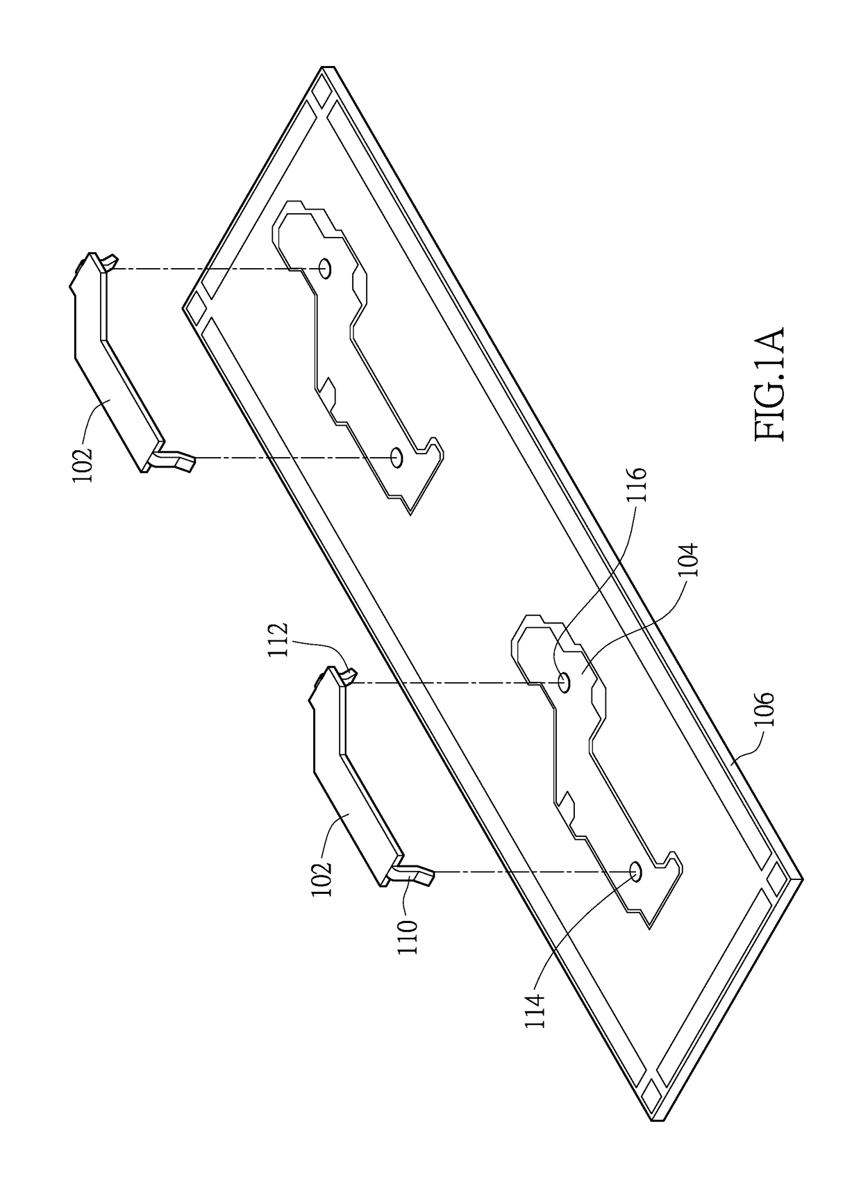
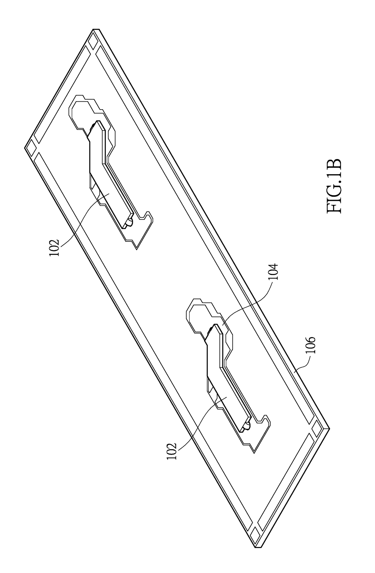
[0026]FIG. 1A shows an exploded view of the printed circuit board of an embodiment of the instant disclosure. FIG. 1B shows a three dimensional view of the printed circuit board at an intermediate stage of an embodiment of the instant disclosure. First, referring to FIG. 1A, the instant disclosure provides a printed circuit board comprising a plate body 106, a conductive pattern 104 disposed on the plate body 106 and a conductive metal plate 102 having a first terminal and a second terminal, and the first terminal and the second terminal of the conductive metal plate 102 are fixed to the plate body 106. Please refer to FIG. 1A and FIG. 1B and also FIG. 2A and FIG. 2B, wherein FIG. 2A shows a plane view of the printed circuit board at an intermediate stage, and FIG. 2B shows a cross section of the printed circuit board at an intermediate stage. The plate body 106 has a first hole 114 and a second hole 116. The first terminal of the conductive metal plate 102 has a first fastening par...

second embodiment

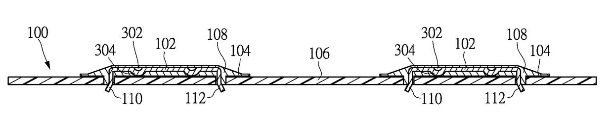
[0029]FIG. 3A shows a three dimensional view of a printed circuit board at an intermediate fabrication stage of the embodiment. FIG. 3B shows a cross section view of a printed circuit board at an intermediate fabrication stage of the embodiment. FIG. 3C shows a cross section view of a printed circuit board at final stage. The difference between this embodiment and the first embodiment is that an accommodating space 306 is formed between the conductive metal plate 102 and the plate body 106. The embodiment uses printing method to form a cavity 302 on the conductive metal plate 102 and form a bump 304 under the conductive metal plate 102. Because the bump 304 abuts against the plate body 106 of the printed circuit board 100, the conductive metal plate 102 is separated from the plate body 106 by a distance to form an accommodating space 306. The other part is like the first embodiment. Like elements use the same symbol and are not described again herein.

[0030]After the conductive metal...

third embodiment

[0031]FIG. 4A shows a cross section view of a printed circuit board at an intermediate fabrication stage of the embodiment. FIG. 4B shows a cross section view of a printed circuit board at final stage of the embodiment. The embodiment is similar to the second embodiment to form an accommodating space 306′ between the conductive metal plate 102′ and the plate body 106, but the difference is that the embodiment uses an arc-shaped conductive metal plate 102′. Because the conductive metal plate 102′ is arc-shaped, after the first fastening part 110 is fastened to the first hole 114 of the plate body 106 and the second fastening part 112 is fastened to the second hole 116 of the plate body 106, the bottom surface of the conductive metal plate 102′ is separated from the top surface of the plate body 106 by a distance. Therefore, an accommodating space 306′ is formed between the conductive metal plate 102′ and the plate body 106. The bottom side of the accommodating space 306′ is a plane, ...


PUM

PropertyMeasurementUnit
voltageaaaaaaaaaa
voltageaaaaaaaaaa
voltageaaaaaaaaaa

Abstract

A printed circuit board is disclosed, comprising a plate body, a conductive pattern disposed on the plate body, a conductive metal plate, and a metal layer. The conductive metal plate has a first terminal and a second terminal, wherein the first terminal and the second terminal are fixed to the plate body. An accommodating space is between the conductive metal plate and the plate body. The metal layer covers the conductive metal plate and the conductive pattern, and is filled into the accommodating space. Therefore, a printed circuit board which has metal blocks with enough thickness is provided. The metal blocks can provide sufficiently low resistance to increase resistance efficiency of the printed circuit.

Description

BACKGROUND OF THE DISCLOSURE[0001]1. Field of the Disclosure[0002]The instant disclosure relates to a printed circuit board; in particular, to a printed circuit board applied with large current.[0003]2. Description of Related Art[0004]Computer equipment has a power supply to transfer input alternating current having voltage 110V or 220V to direct current having voltage 12V or ±5V required by mother boards, hard drives and optical disk drives. As well, power supplies are computer power transferring equipment responsible for transferring alternating current to stable low voltage direct current which can be used by other parts of computers. Because different parts require different voltages, power supplies must provide a plurality of direct voltages to be used by each part of computers.[0005]The power supply has a printed circuit board which is generally called a backboard. Most devices are directly disposed on the backboard, and the current power supply is developed as a large power s...

Claims


Application Information

Patent Timeline
Patent Type & Authority Patents(United States)
IPC IPC(8): H05K1/02H01B5/02H01G5/00
CPCH05K1/0265H05K3/245H05K2201/10272
Inventor FAN, PO-HSIANG
Owner LITE ON ELECTRONICS (GUANGZHOU) LTD
Why Eureka
Try Eureka