Method for manufacturing space transformer by using carrier substrate made for chip package and provided with elongated contacts

a technology of space transformers and carrier substrates, which is applied in the direction of conductive pattern formation, printed element electric connection formation, instruments, etc., can solve the problems of insufficient structural strength of circular contact pads with reduced area, insufficient area and structural strength, and insufficient area

Active Publication Date: 2017-05-09
MPI CORP
View PDF3 Cites 0 Cited by
  • Summary
  • Abstract
  • Description
  • Claims
  • Application Information

AI Technical Summary

Benefits of technology

[0009]The present invention has been accomplished in view of the above-noted circumstances. It is an objective of the present invention to provide a space transformer using a carrier substrate made for a chip package with elongated contacts and a method for manufacturing the same. The space transformer thus obtained has cylindrical contact pads mounted on the elongated contacts of the carrier substrate and having sufficient area and structural strength without short-circuiting adjacent wires.
[0017]As a result, the cylindrical contact pad has so sufficient area and structural strength as to be not easily damaged. Besides, the cylindrical contact pad is separated from the carrier substrate by the insulated layer; therefore, even if the cylindrical contact pad has so large area as to be partially located above the second wire, the first and second wires will not be connected electrically by the cylindrical contact pad and thereby will not be short-circuited.
[0019]Preferably, the aforesaid method comprises a further step of removing a part or a whole of the upper insulated layer after the step (e) so as to expose a peripheral of the cylindrical contact pad partially or completely. That means the space transformer may not have any of the upper insulated layer; alternatively, it may have a part of the upper insulated layer or the whole upper insulated layer so that the cylindrical contact pad of the conductive block is surrounded by the upper insulated layer and thereby strengthened in its structure.

Problems solved by technology

If the carrier substrate made with reduced size for a small chip package has circular contacts with correspondingly reduced size, the circular contacts might be too small to be connected with the chip firmly.
However, the carrier substrate made for the chip package with elongated contacts is difficult to be made as the space transformer of the probe card by the conventional way of mounting large-sized circular contact pads to the original elongated contacts of the carrier substrate due to limit of the very small interval between the adjacent elongated contacts.
That is, the adjacent elongated contacts will be short-circuited by the large-sized circular contact pads unless the area of each circular contact pad is reduced; however, the circular contact pads with reduced area will have insufficient structural strength.

Method used


Image

  • Method for manufacturing space transformer by using carrier substrate made for chip package and provided with elongated contacts
  • Method for manufacturing space transformer by using carrier substrate made for chip package and provided with elongated contacts
  • Method for manufacturing space transformer by using carrier substrate made for chip package and provided with elongated contacts

Examples


Embodiment Construction

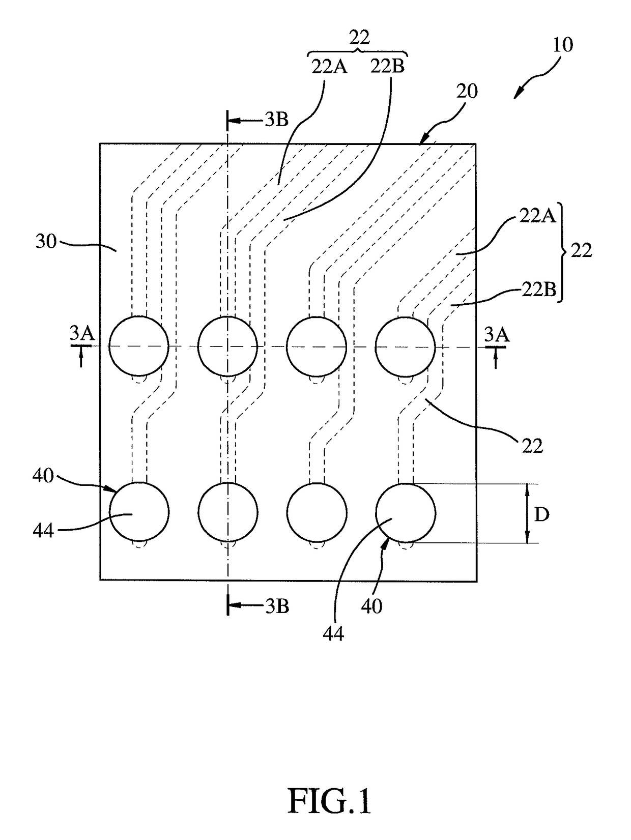
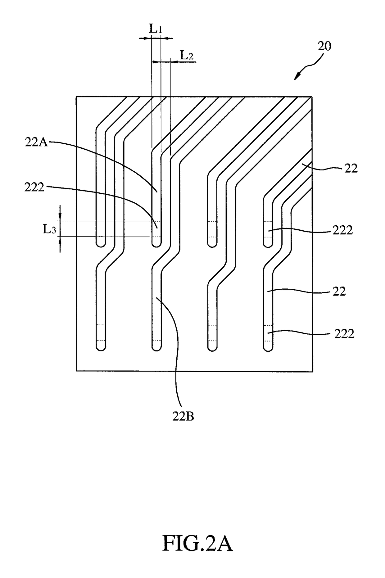
[0033]Referring to FIGS. 1 to 3B, a space transformer 10 according to a first preferred embodiment of the present invention comprises a carrier substrate 20. FIG. 1 is a schematic plane view of a part of the space transformer 10, meaning that the space transformer 10 is not completely shown in FIG. 1. FIG. 2A is a schematic plane view of the carrier substrate 20. FIG. 3A and FIG. 3B are schematic sectional views of the space transformer 10. As shown in FIG. 1, FIG. 3A and FIG. 3B, the space transformer 10 further comprises an insulated layer 30 disposed on the carrier substrate 20, and a plurality of conductive blocks 40 each having at least a part exposed at the outside of the insulated layer 30. It is to be mentioned that FIG. 1, wherein eight conductive blocks 40 are shown, actually illustrates the space transformer 10 partially, as described before; therefore, the amount of the conductive blocks 40 is not limited to that of this embodiment. For the convenience of illustration, o...


PUM

PropertyMeasurementUnit
width L1aaaaaaaaaa
distance L2aaaaaaaaaa
length L3aaaaaaaaaa

Abstract

A method of manufacturing a space transformer includes providing a carrier substrate made for a chip package, forming an insulated layer disposed on the carrier substrate, and forming a conductive block. The carrier substrate is formed with elongated first and second wires. The first wire has an elongated contact which is longer than the width of the first wire. The insulated layer is formed with a hole corresponding in position to the elongated contact. The conductive block is formed with an elongated connecting column located in the hole and connected with the elongated contact, and a cylindrical contact pad exposed at the outside of the insulated layer, larger-sized than the elongated connecting column is connected with the elongated connecting column. As a result, the cylindrical contact pad has sufficient area and structural strength for contact with a probe needle.

Description

BACKGROUND OF THE INVENTION[0001]1. Field of the Invention[0002]The present invention relates generally to space transformers for being used in probe cards and more particularly, to a space transformer using a carrier substrate which is originally made for a chip package and provided with elongated contacts, and to a method for manufacturing the space transformer.[0003]2. Description of the Related Art[0004]A probe card usually comprises a main circuit board adapted to be electrically connected with signal-transmitting contacts of a testing apparatus directly, and a space transformer (hereinafter referred to as “ST”) mounted to a bottom surface of the main circuit board. The space transformer is provided at a top surface thereof with a plurality of top contact pads adapted for being electrically connected with the main circuit board, and at a bottom surface thereof with a plurality of bottom contact pads adapted for being connected with a plurality of probe needles, such as vertical...

Claims


Application Information

Patent Timeline
Patent Type & Authority Patents(United States)
IPC IPC(8): H05K3/40G01R3/00H05K3/14H05K3/10H05K3/32G01R1/067G01R1/20H01R43/20G01R1/073
CPCH05K3/4007G01R1/067G01R1/20G01R3/00H01R43/20H05K3/10H05K3/143H05K3/32H05K3/403H05K3/4038G01R1/07378H05K2201/09409H05K2203/0574H05K2203/1476Y10T29/49147Y10T29/49162Y10T29/49165
Inventor LEE, CHUNG-TSEWU, CHIEN-CHOUCHEN, TSUNG-YI
Owner MPI CORP
Why Eureka
Try Eureka