
Low resistance contacts for semiconductor devices

a technology of low resistance and contacts, applied in semiconductor devices, semiconductor/solid-state device details, electrical devices, etc., can solve the problems of high contact resistance to n-type ge layers, process variability can arise from rough or unintentional textured surfaces, and achieve the effect of minimizing leakage currents

Active Publication Date: 2017-03-28
LASER SYST & SOLUTIONS OF EURO LASSE SCREEN SEMICON SOLUTIONS CO LTD +1
View PDF6 Cites 0 Cited by
  • Summary
  • Abstract
  • Description
  • Claims
  • Application Information

AI Technical Summary

Benefits of technology

The patent text describes a method for making semiconductor devices using a process called laser thermal annealing (LTA). The method is compared to conventional methods and is found to have several advantages, including better surface topography, better interface quality, and better crystal structure. The use of LTA also simplifies the overall process by allowing annealing in ambient air. The method also includes steps to minimize leakage currents. Overall, the patent text describes a more efficient and effective method for making semiconductor devices.

Problems solved by technology

A remaining stumbling block to the association of Germanium (Ge) with production processes of advanced logic devices, is the high contact resistance to n-type Ge layers.
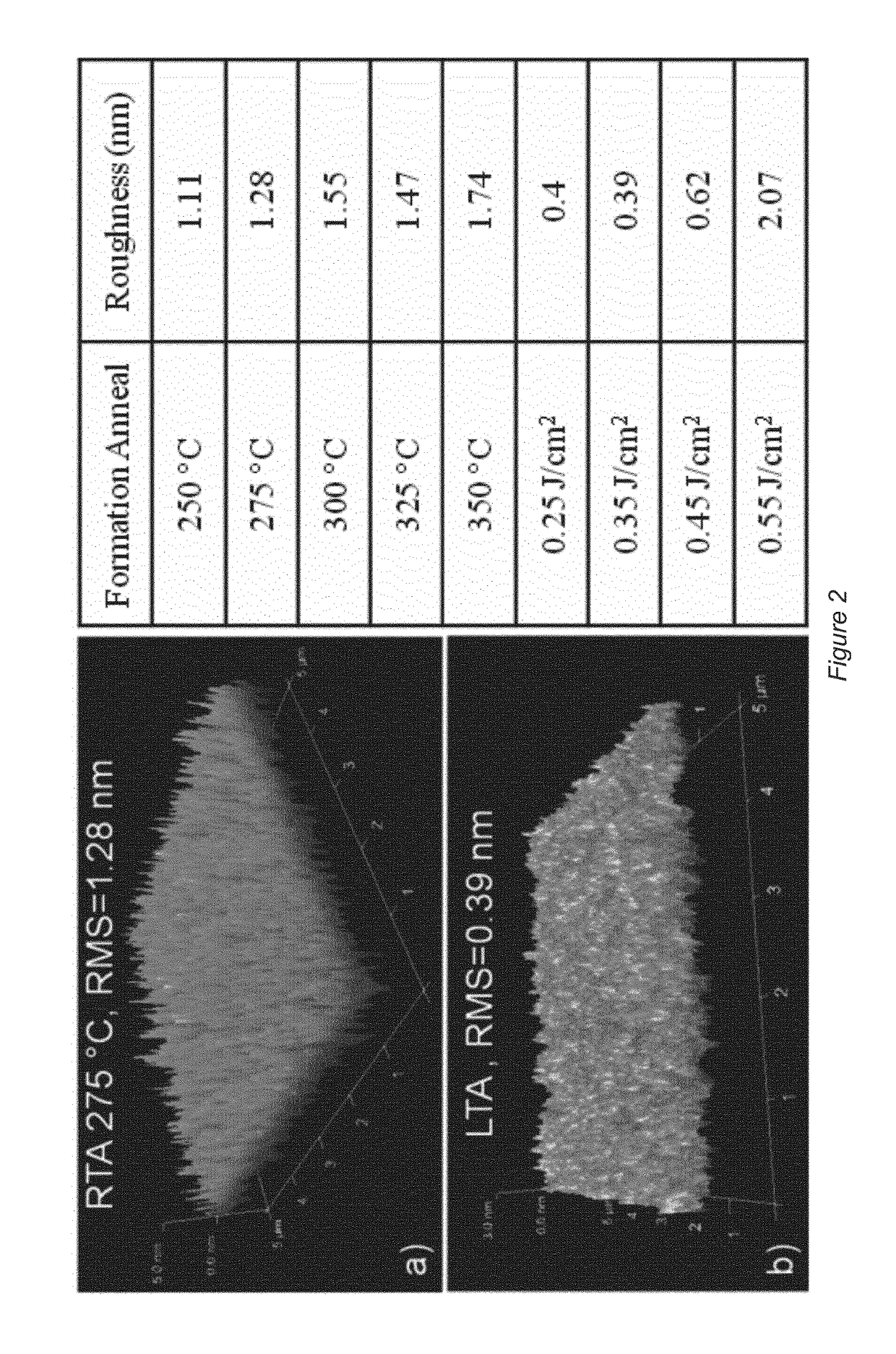
High resistance may arise from poor quality contacts, process variability can arise from rough or unintentionally textured surfaces.
Specifically in Ge, the n-type system has proven difficult because of the large electron Schottky barrier height (eSBH) and resulting high contact resistance (ρc), and surface states associated with dangling bonds at the Ge surface can lead to Fermi-Level Pinning (FLP) [1, 2].
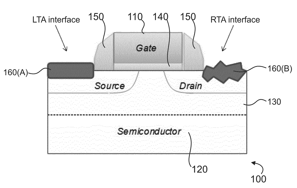
This results in a relatively rough interface between the NiGe layer and the Ge underneath.
However, the NiGe interface with the underlying substrate was not smooth.

Method used


Image

  • Low resistance contacts for semiconductor devices
  • Low resistance contacts for semiconductor devices
  • Low resistance contacts for semiconductor devices

Examples


Embodiment Construction

[0052]There will now be described by way of example a specific mode contemplated by the inventors. In the following description numerous specific details are set forth in order to provide a thorough understanding. It will be apparent however, to one skilled in the art, that the present invention may be practiced without limitation to these specific details. In other instances, well known methods and structures have not been described in detail so as not to unnecessarily obscure the description.

[0053]Laser Thermal Annealing (LTA) is used to form Germanide contacts on n-doped Ge, which are systematically compared to results generated by conventional rapid thermal annealing (RTA). Surface topography, interface quality, crystal structure, and material stoichiometry are explored for both annealing techniques. For electrical characterization, specific contact resistivity and thermal stability are extracted. It is shown that LTA can produce a uniform contact with a remarkably smooth substr...


PUM


Abstract

The invention provides a method of forming at least one Metal Germanide contact on a substrate for providing a semiconducting device (100) by providing a first layer (120) of Germanium (Ge) and a second layer of metal. The invention provides a step of reacting the second layer with the first layer with high energy density pulses for obtaining a Germanide metal layer (160A) having a substantially planar interface with the underlying first (Ge) layer.

Description

CROSS REFERENCE TO RELATED APPLICATIONS[0001]This is the national phase under 35 U.S.C. §371 of International Application No. PCT / EP2014 / 051782, filed on Jan. 30, 2014, which claims priority to and the benefit of European Patent Application No. 13153312.7, filed on Jan. 30, 2013 and U.S. Patent Application No. 61 / 758,716, filed on Jan. 30, 2013, the entire disclosures of each of which are incorporated by reference herein.FIELD OF THE INVENTION[0002]The present invention relates to improvements in low resistance contacts for semiconductor devices. In particular, the present invention relates to a method of providing semiconductor device transistors with improved low resistance contacts.BACKGROUND OF THE INVENTION[0003]Germanium (Ge) is a promising material for advanced semiconductor devices, because it provides much higher carrier mobilities than Silicon (Si). A remaining stumbling block to the association of Germanium (Ge) with production processes of advanced logic devices, is the ...

Claims


Application Information

Patent Timeline
Patent Type & Authority Patents(United States)
IPC IPC(8): H01L23/52H01L21/324H01L21/268H01L29/45H01L29/16H01L29/08H01L29/78H01L21/285
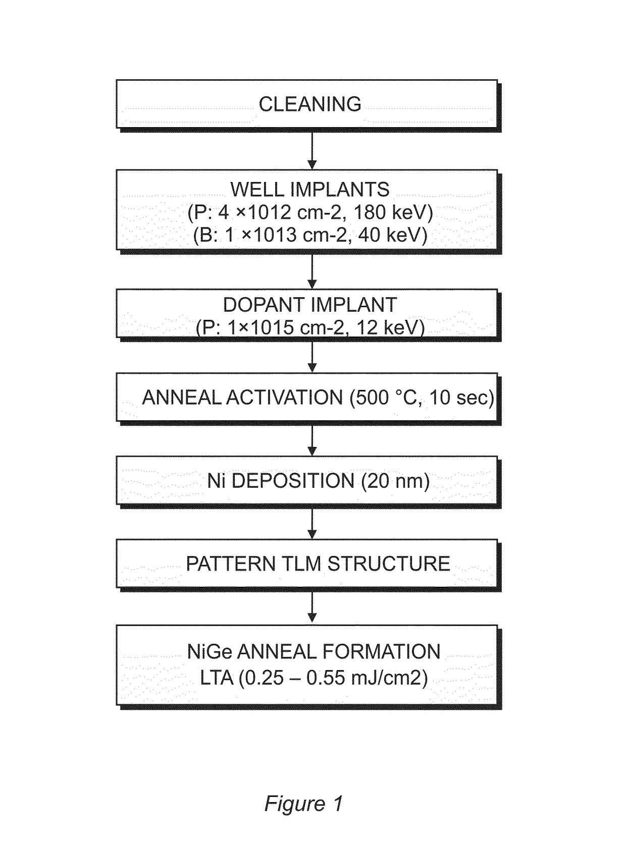
CPCH01L21/3247H01L21/268H01L21/2855H01L21/28512H01L21/28568H01L21/324H01L29/0847H01L29/16H01L29/45H01L29/78
Inventor DUFFY, RAYSHAYESTEH, MARYAMHUET, KARIM
Owner LASER SYST & SOLUTIONS OF EURO LASSE SCREEN SEMICON SOLUTIONS CO LTD
Learn More