Liquid crystal display device

a display device and liquid crystal technology, applied in the field of liquid crystal display devices, can solve the problems of difficult control of the distribution of charges accumulated on the counter substrate, hardly influence on the display of images, and variations in luminance, so as to prevent local application of voltage, prevent the change of the potential of the pixel electrode or the common electrode, and prevent the effect of local application of voltag

Active Publication Date: 2017-02-28
SEMICON ENERGY LAB CO LTD
View PDF37 Cites 7 Cited by
  • Summary
  • Abstract
  • Description
  • Claims
  • Application Information

AI Technical Summary

Benefits of technology

[0010]Furthermore, since the capacitive touch panel obtains positional information by sensing a slight change in capacitance between electrodes included in the touch panel or between these electrodes and a conductive object such as a finger, a change in the potential of a signal that is necessary for operation of the liquid crystal panel might appear as a noise and adversely affect the obtainment of the positional information in the touch panel. In particular, in the in-cell liquid crystal display device including a touch panel, the distance between the element substrate on which a transistor is formed and a wiring or electrode of the touch panel is shorter than that in the on-cell liquid crystal display device including a touch panel and thus the parasitic capacitance generated between the wiring or electrode of the touch panel and a wiring or electrode included in the liquid crystal panel tends to be larger. Accordingly, the in-cell liquid crystal display device including a touch panel has a high possibility that a change in the potential of a signal that is necessary for operation of the liquid crystal panel appears as a noise and causes an adverse effect in obtaining positional information in the touch panel, as compared with the on-cell liquid crystal display device including a touch panel.
[0011]Moreover, the distance between the electrodes for obtaining the positional information and the conductive object such as a finger is longer in the in-cell liquid crystal display device including a touch panel than in the on-cell liquid crystal display device including a touch panel. Therefore, the in-cell liquid crystal display device including a touch panel has a lower sensitivity in obtaining positional information and a smaller signal-to-noise ratio (SN ratio).
[0016]In one embodiment of the present invention, the pair of electrodes is positioned on the second substrate side, and charges accumulated on the second substrate can be discharged through one of the pair of electrodes. This prevents accumulation of charges on part of the second substrate, thereby preventing local application of voltage to the liquid crystal layer. Thus, variations in luminance can be prevented.
[0017]In one embodiment of the present invention, since the conductive film exists between the pixel electrode and the common electrode positioned on the first substrate side and the pair of electrodes positioned on the second substrate side, a parasitic capacitance is generated between the pixel electrode or the common electrode and the conductive film, and another parasitic capacitance is generated between the pair of electrodes and the conductive film. By application of a predetermined potential to the conductive film in the state where the parasitic capacitances are generated as described above, a change in the potential of the pair of electrodes can be prevented even when the potential applied to the pixel electrode is changed. In addition, a change in the potential of the pixel electrode or the common electrode can be prevented even when the potential of the pair of electrodes is changed at the time of obtaining positional information. Thus, in the in-cell liquid crystal display device of one embodiment of the present invention, a change in the potential of a signal that is necessary for operation of the liquid crystal panel is prevented from appearing as a noise and causing an adverse effect in obtaining positional information in the touch panel.
[0018]With one embodiment of the present invention, a liquid crystal display device including a touch panel and having small variations in luminance, can be provided. Further, with one embodiment of the present invention, a liquid crystal display device that is not influenced by a noise in obtaining positional information can be provided.

Problems solved by technology

Therefore, in the case where a horizontal electric field mode liquid crystal panel in which horizontal electric field is applied to liquid crystal is used in a liquid crystal display device including a touch panel, a press hardly influences display of images.
However, the horizontal electric field mode liquid crystal panel does not include an electrode on a counter substrate that faces an element substrate on which a transistor is provided.
This makes it difficult to control the distribution of charges accumulated on the counter substrate.
In some cases, many charges might be accumulated on part of the counter substrate by the influence of static electricity, and the accumulated charges make excessive electric field applied locally to liquid crystal, causing variations in luminance.
Furthermore, since the capacitive touch panel obtains positional information by sensing a slight change in capacitance between electrodes included in the touch panel or between these electrodes and a conductive object such as a finger, a change in the potential of a signal that is necessary for operation of the liquid crystal panel might appear as a noise and adversely affect the obtainment of the positional information in the touch panel.
Accordingly, the in-cell liquid crystal display device including a touch panel has a high possibility that a change in the potential of a signal that is necessary for operation of the liquid crystal panel appears as a noise and causes an adverse effect in obtaining positional information in the touch panel, as compared with the on-cell liquid crystal display device including a touch panel.

Method used


Image

  • Liquid crystal display device
  • Liquid crystal display device
  • Liquid crystal display device

Examples


Embodiment Construction

[0034]Embodiment of the present invention will be described below in detail with reference to the drawings. Note that the present invention is not limited to the following description, and it is easily understood by those skilled in the art that the mode and details can be variously changed without departing from the spirit and scope of the present invention. Therefore, the present invention should not be construed as being limited to the description of the embodiments below.

[0035]Note that in this specification, the category of a liquid crystal display device includes a panel in which liquid crystal elements are formed in respective pixels, and a module in which an IC or the like including a driver circuit or a controller is mounted on the panel.

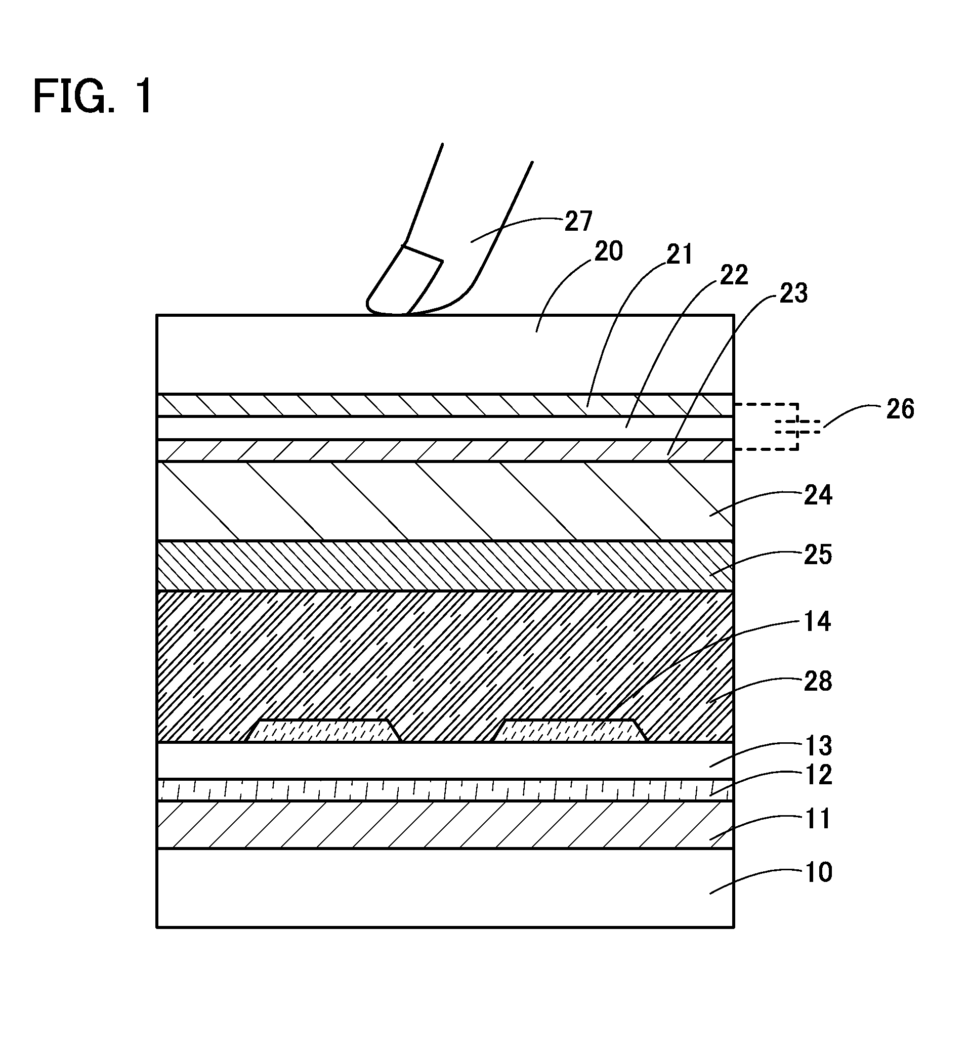
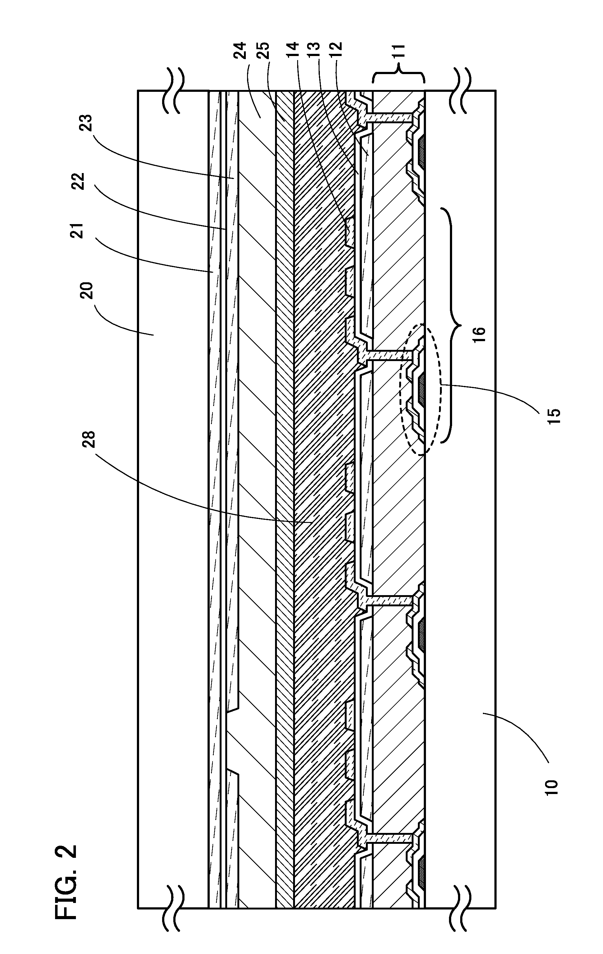
[0036]FIG. 1 illustrates an example of a stacked structure of a pixel in a liquid crystal display device of one embodiment of the present invention.

[0037]The liquid crystal display device of one embodiment of the present invention includes,...


PUM

PropertyMeasurementUnit
relative dielectric constantaaaaaaaaaa
pressureaaaaaaaaaa
temperatureaaaaaaaaaa

Abstract

A liquid crystal display device that is not influenced by a noise in obtaining positional information can be provided. The liquid crystal display device includes a first substrate provided with a pixel electrode and a common electrode with a first insulating film interposed therebetween. The pixel electrode and the common electrode partly overlap with each other. The liquid crystal display device further includes a second substrate provided with a pair of electrodes, a resin film covering the pair of electrodes, and a conductive film on the resin film. The pair of electrodes partly overlap with each other with a second insulating film interposed therebetween. The liquid crystal display device further includes a liquid crystal layer between the conductive film on the second substrate side and the pixel electrode and the common electrode on the first substrate side. A predetermined potential is supplied to the conductive film.

Description

BACKGROUND OF THE INVENTION[0001]1. Field of the Invention[0002]The present invention relates to liquid crystal display devices. In particular, the present invention relates to liquid crystal display devices having a touch panel function.[0003]2. Description of the Related Art[0004]A touch panel functions as a position input device that can detect a position indicated with a finger, a stylus, or the like to generate a signal including the positional information. A capacitive touch panel can obtain positional information without being influenced by external light, unlike an optical touch panel such as an infrared touch panel. Furthermore, the capacitive touch panel can obtain the positional information at high speed as compared with a resistive touch panel and does not cause physical wear of electrodes. For these reasons, capacitive touch panels have come into wide use in the market in recent years.[0005]In addition, as the kinds of liquid crystal display devices including a touch pa...

Claims


Application Information

Patent Timeline
Patent Type & Authority Patents(United States)
IPC IPC(8): G02F1/1333G02F1/1368G02F1/1337G06F3/041
CPCG02F1/13338G06F3/0412G02F2001/133334G06F2203/04103G06F3/0446G02F1/133334G02F1/136286G02F1/133509G02F1/1343G02F1/133345G02F1/1337G02F1/134309G02F1/1368G02F1/137G02F2201/121G02F2201/123
Inventor TANABE, TORUFUKUTOME, TAKAHIROMORIYA, KOJIKUROSAKI, DAISUKEOHNO, MASAKATSU
Owner SEMICON ENERGY LAB CO LTD
Why Eureka
Try Eureka