Supercomputer using wafer scale integration

a supercomputer and wafer technology, applied in the field of mass-parallel supercomputers, can solve the problems of limited number of electrical connections between chips, limited bisectional bandwidth between separate processor chips in a supercomputer, and limited individual chip siz

Active Publication Date: 2017-02-14
INT BUSINESS MASCH CORP
View PDF9 Cites 2 Cited by
  • Summary
  • Abstract
  • Description
  • Claims
  • Application Information

AI Technical Summary

Benefits of technology

[0005]According to an embodiment of the disclosure, there is provided a semiconductor structure that includes a substrate that includes one or more cooling layers, one or more cooling channels, one or more coolant inlets and outlets in fluid communication with the cooling channels, a device layer disposed on the cooling layers that has one or more connection points and a device layer area, wherein a device layer thermal coefficient of expansion is substantially equal to that of the one or more cooling layers, a plurality of laminate substrates arranged in an array that are disposed on, and electrically attached to, the device layer, wherein a laminate substrate thermal coefficient of expansion differs from that of the device layer, and each laminate substrate is smaller in area than an area of the device layer portion to which it is attached, and each laminate substrate includes sides with gaps between sides of adjacent laminate substrates, wherein the laminate substrates are not electrically or mechanically connected to each other across the gaps between laminate substrates and the laminate substrates are small enough to substantially prevent warping and unacceptable stress of the device layer, interconnection and cooling layers due to thermal expansion.

Problems solved by technology

The bisectional bandwidth between separate processor chips in a supercomputer is typically limited by the speed and number of electrical links which can be provided between the processors.
The size of individual chips is limited by lithographic field size, yield, and chip packaging technology, and the number of electrical connections between chips is also limited by chip packaging technology.
A number of useful computational tasks can be limited by the available bisectional bandwidth, such as sparse matrix multiplication used in natural language processing, or large fast Fourier transforms (FFTs).

Method used


Image

  • Supercomputer using wafer scale integration
  • Supercomputer using wafer scale integration
  • Supercomputer using wafer scale integration

Examples


Embodiment Construction

[0031]Exemplary embodiments of the disclosure as described herein generally include supercomputers fabricated using wafer-scale integration, and methods for fabricating the same. Accordingly, while embodiments of the disclosure are susceptible to various modifications and alternative forms, specific embodiments thereof are shown by way of example in the drawings and will herein be described in detail. It should be understood, however, that there is no intent to limit embodiments of the disclosure to the particular exemplary embodiments disclosed, but on the contrary, embodiments of the disclosure cover all modifications, equivalents, and alternatives falling within the spirit and scope of the disclosure.

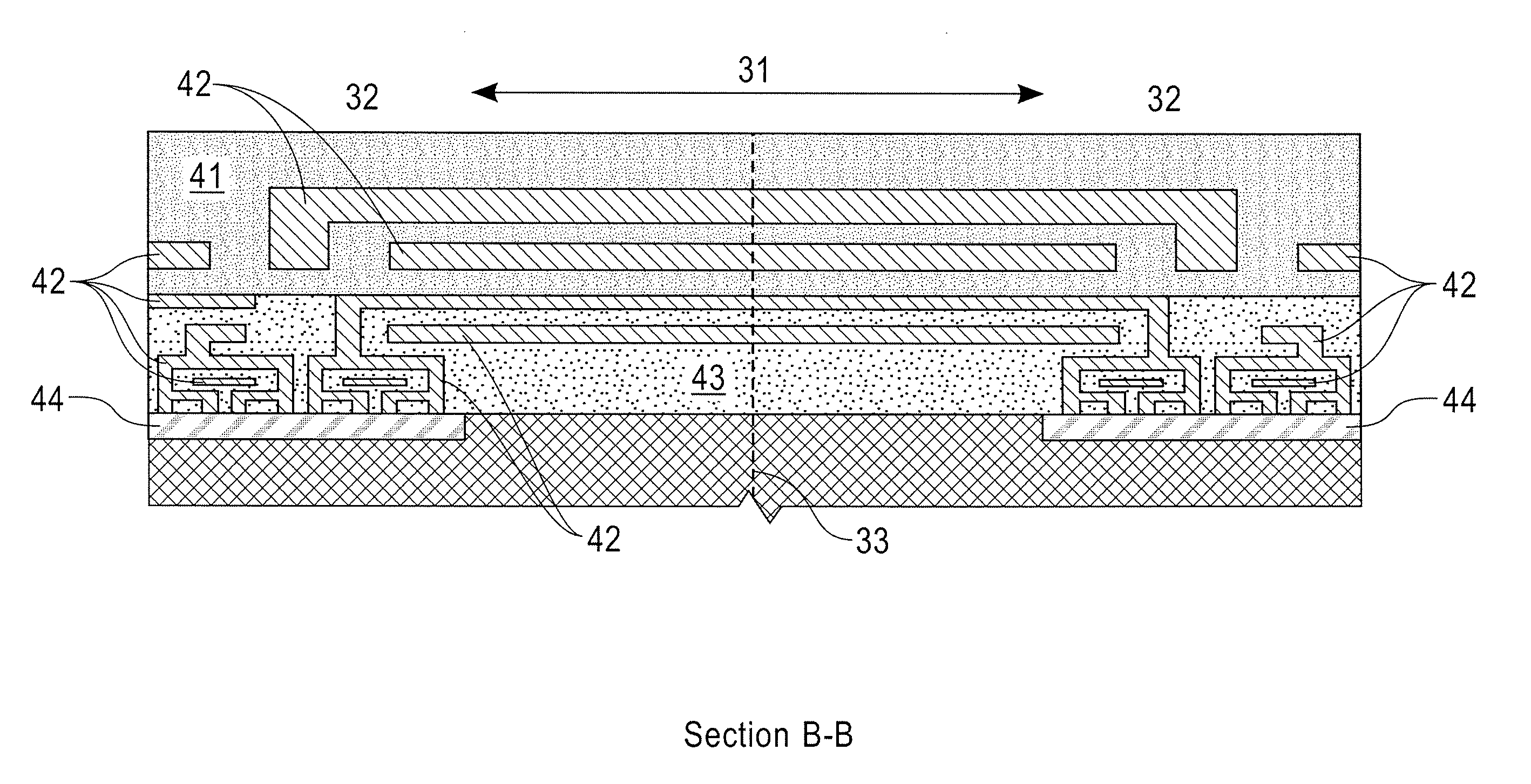
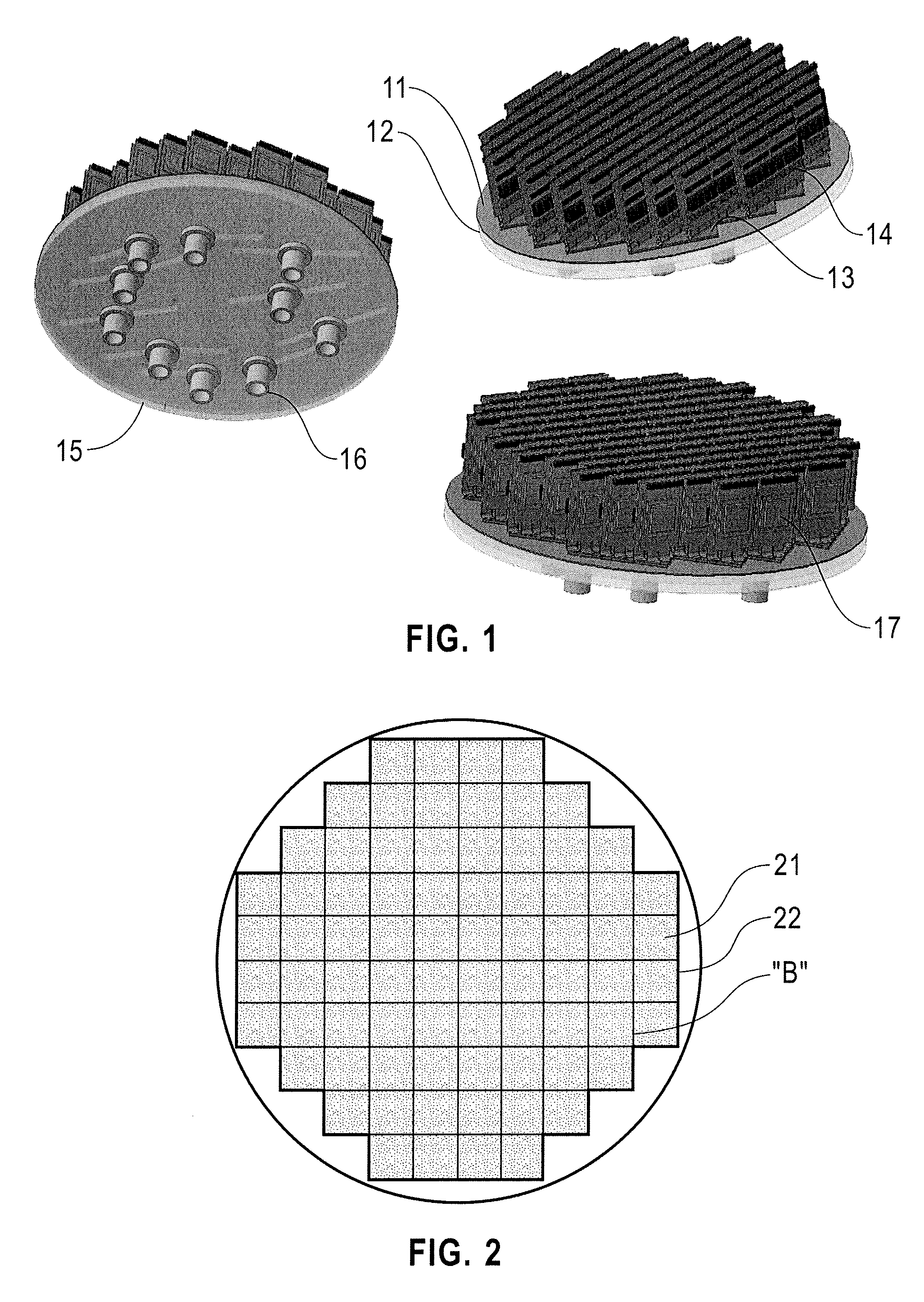
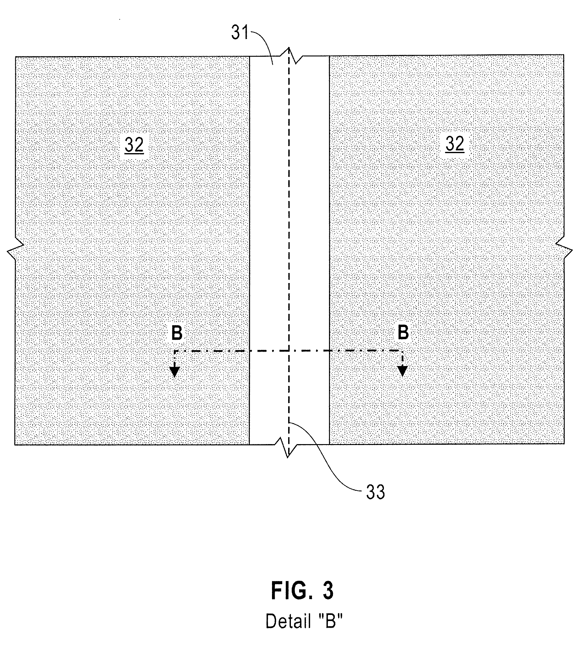
[0032]Exemplary embodiments of the present disclosure include a wafer whose surface is fully populated with chips composed of many small processors that are electrically interconnected using the upper levels of chip wiring, a connection scheme known as wafer scale integration. Chip t...


PUM


Abstract

A semiconductor structure includes a substrate with cooling layers, cooling channels, coolant inlets and outlets in fluid communication with the cooling channels, and a device layer on the cooling layers with one or more connection points and a device layer area. The device layer thermal coefficient of expansion is substantially equal to that of the cooling layers. A plurality of laminate substrates are disposed on, and electrically attached to, the device layer. The laminate substrate thermal coefficient of expansion differs from that of the device layer, each laminate substrate is smaller than the device layer portion to which it is attached, and each laminate substrate includes gaps between sides of adjacent laminate substrates. The laminate substrates are not electrically or mechanically connected to each other across the gaps therebetween and the laminate substrates are small enough to prevent warping of the device, interconnection and cooling layers due to thermal expansion.

Description

BACKGROUND[0001]Technical Field[0002]Embodiments of the present disclosure are directed to massively parallel supercomputers made from multi-core processor chips.[0003]Discussion of the Related Art[0004]Contemporary supercomputers typically use thousands of processors that are either distributed across a network or are placed in close proximity to each other as in a centralized computer cluster. More recently, supercomputers have started using multi-core processors, with the idea of developing a supercomputer on a chip. The bisectional bandwidth between separate processor chips in a supercomputer is typically limited by the speed and number of electrical links which can be provided between the processors. The available bandwidth between processors on the same chip is significantly higher than what can typically be provided between processors on different chips. The size of individual chips is limited by lithographic field size, yield, and chip packaging technology, and the number of...

Claims


Application Information

Patent Timeline
Patent Type & Authority Patents(United States)
IPC IPC(8): H01L23/473H01L23/498G06F1/18G06F1/20H01L23/367
CPCG06F1/185G06F1/20H01L23/367H01L23/473H01L23/49816H01L23/49838H01L2224/92242H01L24/94H01L24/97H01L25/50H01L2224/04026H01L2224/05644H01L2224/05655H01L2224/05666H01L2224/13109H01L2224/13116H01L2224/16227H01L2224/24137H01L2224/29116H01L2224/2919H01L2224/32225H01L2224/73204H01L2224/73253H01L2224/81805H01L2224/92125H01L2224/94H01L2224/97H01L2924/1431H01L2924/1434H01L2924/157H01L2924/15787H01L2924/15788H01L2224/05583G06F2200/201H01L2224/83H01L2924/0105H01L2224/81H01L2224/16225H01L2924/00
Inventor COLGAN, EVAN G.DENNEAU, MONTY M.KNICKERBOCKER, JOHN
Owner INT BUSINESS MASCH CORP
Why Eureka
Try Eureka