Display device
a display device and substrate technology, applied in the field of display devices, can solve the problems of substrate or a wiring provided over the substrate being destroyed, connection wiring peeling from the substrate, etc., and achieve the effect of high-reliability display devices
- Summary
- Abstract
- Description
- Claims
- Application Information
AI Technical Summary
Benefits of technology
Problems solved by technology
Method used
Image
Examples
embodiment 1
[0035]In this embodiment, configuration examples of a display device of one embodiment of the present invention will be described with reference to drawings.
[Configuration Example of Display Device]
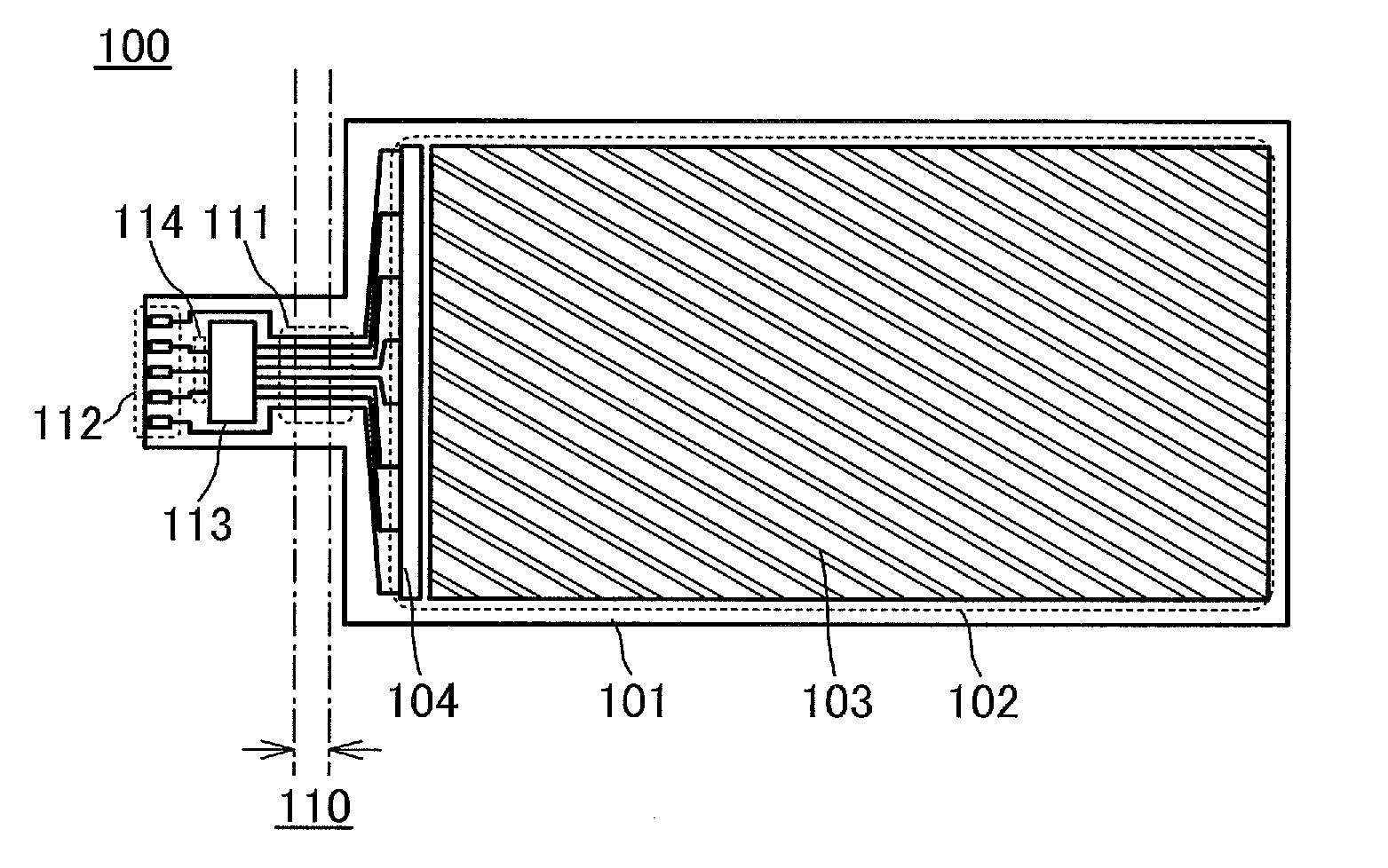
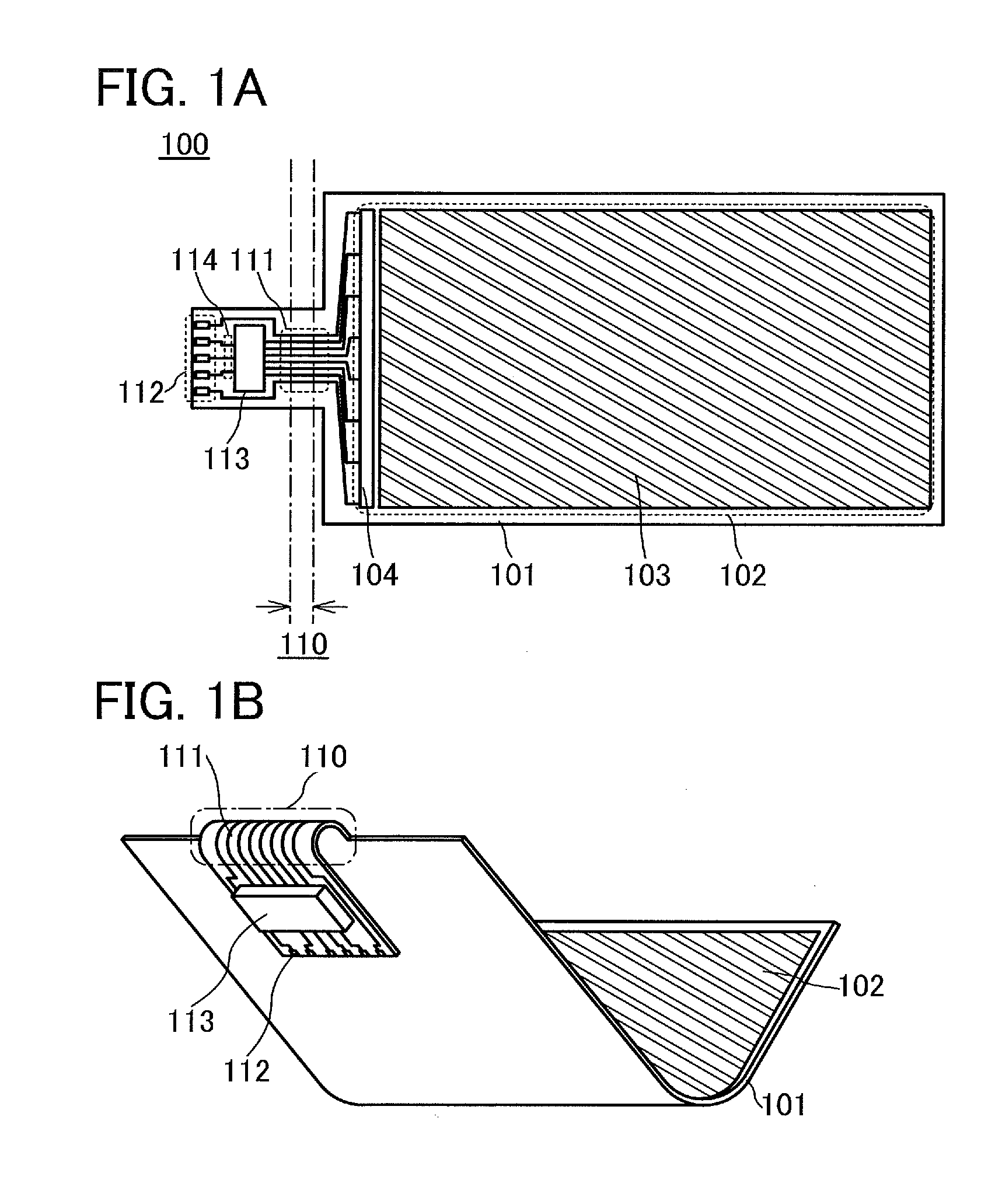
[0036]FIG. 1A is a schematic top view of a display device 100 of one embodiment of the present invention.
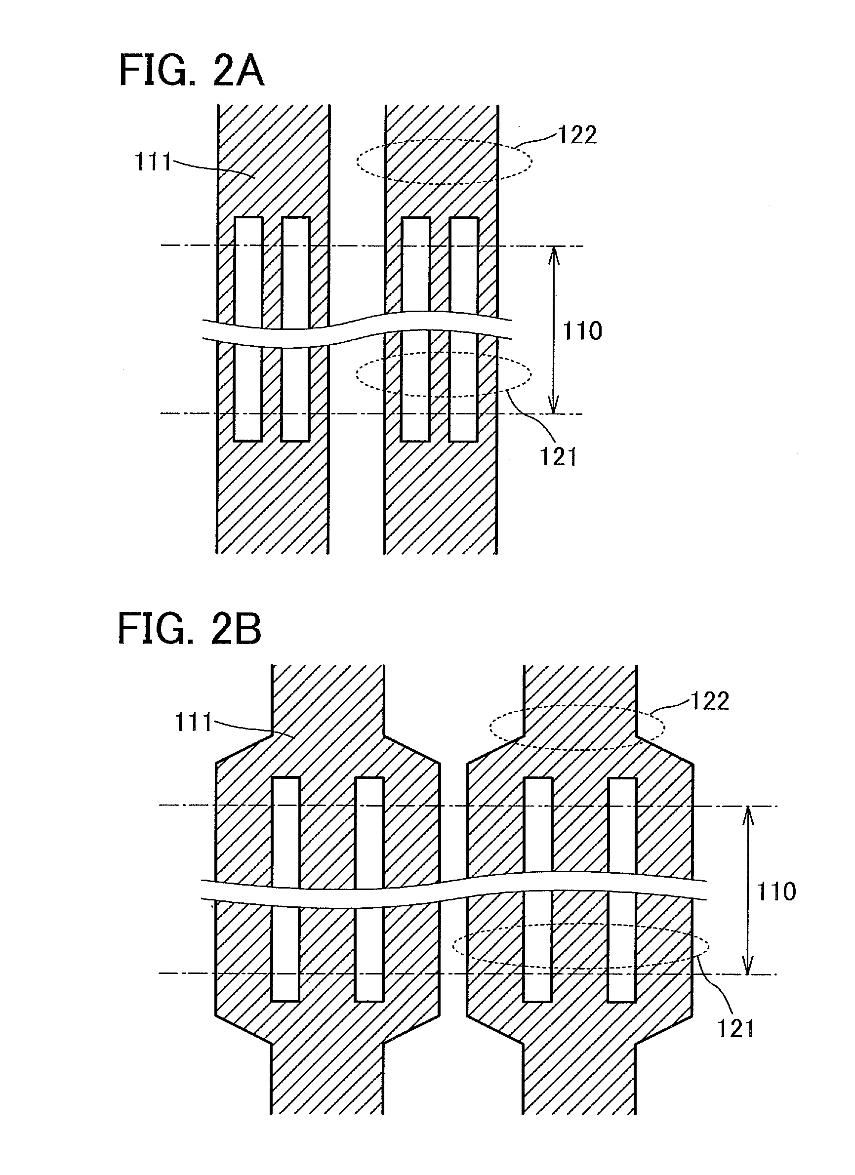
[0037]The display device 100 includes a display portion 102, a plurality of wirings 111, a plurality of connection terminals 112, an IC 113, and a plurality of wirings 114 over a flexible substrate 101.
[0038]The display portion 102 includes a pixel portion 103 and a driver circuit 104.
[0039]In the pixel portion 103, pixels each including a display element are arranged in a matrix. By driving each pixel, an image can be displayed on the pixel portion 103.
[0040]As a display element that can be used in a pixel, an organic electroluminescence (EL) element, a liquid crystal element, or the like can be used. Alternatively, an element that performs display by an electrophoretic method, an ele...
embodiment 2
[0115]An example of a method for manufacturing a display device of one embodiment of the present invention will be described below.
[Example of Manufacturing Method]
[0116]First, a separation layer 202 is formed over a supporting substrate 201.
[0117]As the supporting substrate 201, a substrate having heat resistance to at least the heat applied in a subsequent process is used. Examples of the supporting substrate 201 include a glass substrate, a resin substrate, a semiconductor substrate, a metal substrate, and a ceramic substrate.
[0118]As a material of the separation layer 202, a high melting point metal material such as tungsten, titanium, or molybdenum can be used, for example. Tungsten is preferably used.
[0119]The separation layer 202 can be formed by a sputtering method, for example.
[0120]Then, a separation layer 203 is formed over the separation layer 202. An oxide layer 211 is formed between the separation layer 202 and the separation layer 203.
[0121]As a material of the separa...
embodiment 3
[0165]In this embodiment, specific configuration examples of the display device described in Embodiment 1 will be described with reference to drawings. Examples of an image display device to which an organic EL element is used will be described below.
[Configuration Example 1 of Display Device]
[0166]FIG. 9 is a schematic cross-sectional view of a display device 300 with a top emission structure. The schematic top view of the display device 300 of FIG. 9 corresponds to FIG. 1A, and FIG. 9 corresponds to a schematic cross-sectional view of the region including the display portion 102, the wiring 111, and the connection terminal 112 in FIGS. 1A and 1B.
[0167]The display device 300 includes the separation layer 203 over a flexible substrate 354 with an adhesive layer 135 interposed therebetween. The display device 300 further includes, over the separation layer 203, the pixel portion 103 including a light-emitting element 340, the driver circuit 104, the wiring 111, and the connection ter...
PUM
 Abstract
Description
Claims
Application Information
 - R&D
- Intellectual Property
- Life Sciences
- Materials
- Tech Scout
- Unparalleled Data Quality
- Higher Quality Content
- 60% Fewer Hallucinations
Browse by: Latest US Patents, China's latest patents, Technical Efficacy Thesaurus, Application Domain, Technology Topic, Popular Technical Reports.
© 2025 PatSnap. All rights reserved.Legal|Privacy policy|Modern Slavery Act Transparency Statement|Sitemap|About US| Contact US: help@patsnap.com


