
Thin film transistor array panel

a transistor array and thin film technology, applied in the field of thin film transistor array panels, can solve the problems of disadvantageous viewing angle of birefringence (ecb) lcds, and achieve the effects of increasing the aperture ratio, reducing the kickback voltage, and high resolution performan

Inactive Publication Date: 2016-10-11
SAMSUNG DISPLAY CO LTD
View PDF8 Cites 0 Cited by
  • Summary
  • Abstract
  • Description
  • Claims
  • Application Information

AI Technical Summary

Benefits of technology

[0035]According to embodiments of the inventive concept, a thin film transistor array panel is capable of decreasing an entire area of a thin film transistor, thereby increasing an aperture ratio and achieving high resolution performance.
[0036]Further, according to embodiments of the inventive concept, a thin film transistor array panel is capable of decreasing kickback voltage, thereby reducing voltage ripple and image sticking and thus achieving high resolution performance.

Problems solved by technology

Therefore, twisted nematic (TN), patterned vertical alignment (PVA) and electrically controlled birefringence (ECB) LCDs have disadvantageously a smaller viewing angle due to refractive index anisotropy of liquid crystal molecules when voltage is applied.

Method used


Image

  • Thin film transistor array panel
  • Thin film transistor array panel
  • Thin film transistor array panel

Examples


first embodiment

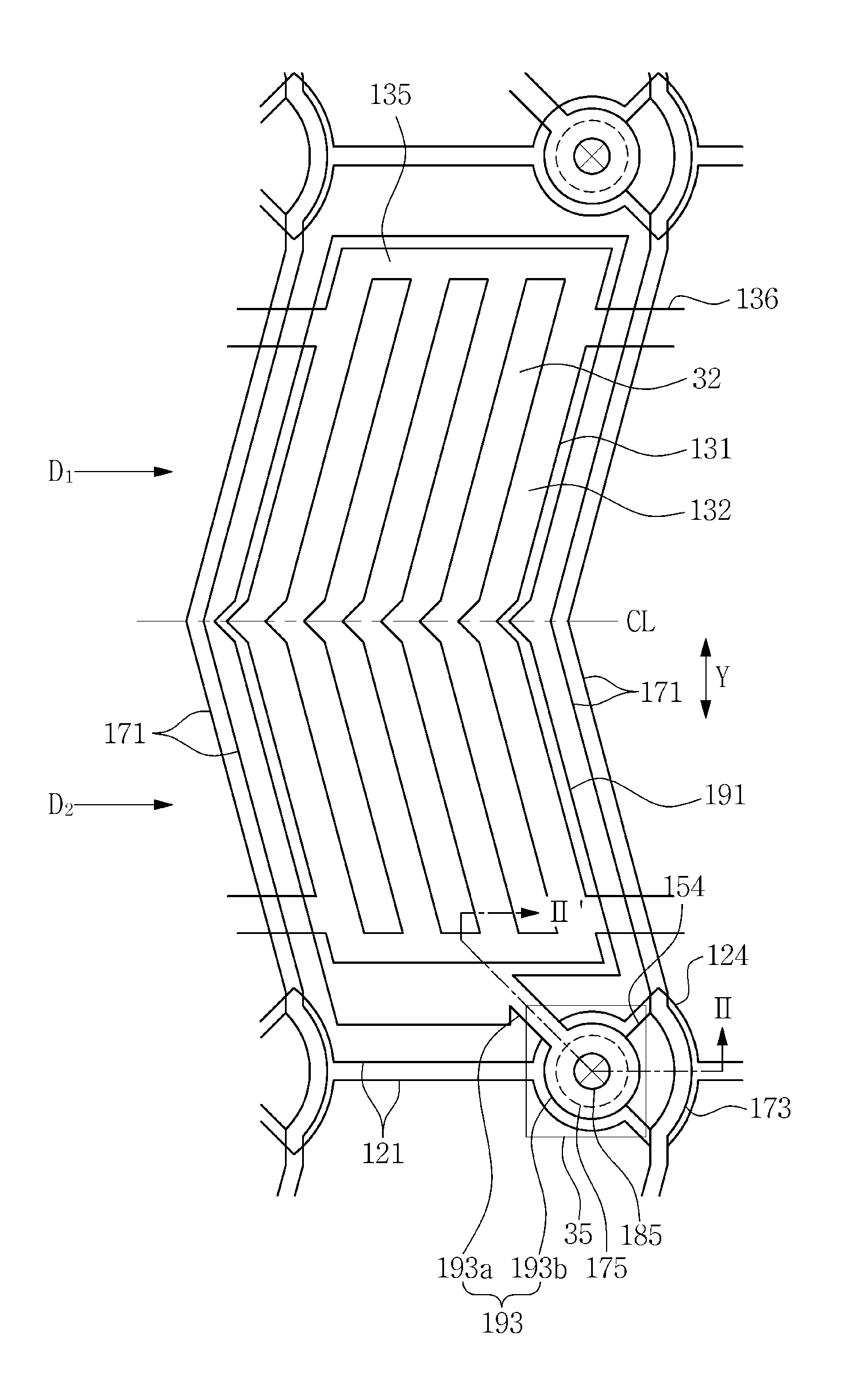
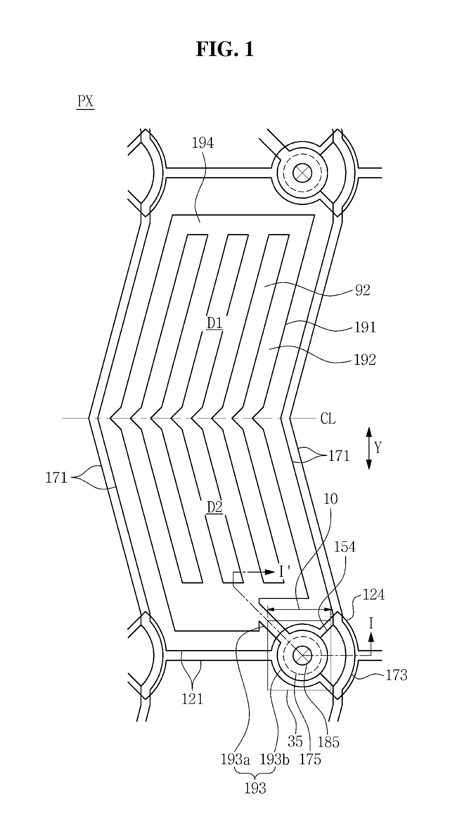
[0055]FIG. 1 is a schematic plan view illustrating a display device according to the inventive concept; and FIG. 2 is a cross-sectional view taken along line I-I′ of FIG. 1

[0056]Referring to FIGS. 1 and 2, and in particular to FIG. 2 initially, the LCD according to the first embodiment includes lower and upper array panels 100 and 200 that face (or oppose) each other and also includes a liquid crystal layer 30 interposed between the lower and upper array panels 100 and 200.

[0057]First, the upper array panel 200 will be described as follows.

[0058]A light blocking member 220 and a color filter 230 may be disposed on a substrate 210 including transparent glass or plastic. The light blocking member 220 is also called a black matrix and may be configured to prevent or reduce light leakage between pixels PX. The color filter 230 may display one of three primary colors, i.e., red, green, and blue. At least one of the light blocking member 220 and the color filter 230 may be disposed on the...

fourth embodiment

[0117]FIG. 9 is a schematic plan view illustrating a display device according to the inventive concept.

[0118]Referring to FIG. 9, the plurality of branch electrodes 192 of the first electrode 191, the slit 92, and the data line 171 may not be inclined at an oblique angle with respect to the vertical direction (Y) but may be disposed in a straight manner. In view of manufacturing costs and process efficiency, the first electrode 191 may be shaped (or formed) as in the first or fourth exemplary embodiment.

[0119]Hereinafter, a fifth exemplary embodiment of the inventive concept will be described with reference to FIGS. 10 and 11. The fifth exemplary embodiment is almost similar to the first exemplary embodiment in terms of configuration, but there are differences in a shape of the first electrode 191 and a position where the second electrode 131 is laminated. For ease of description, the fifth exemplary embodiment will be described herein based on the differences between the two exempl...


PUM


Abstract

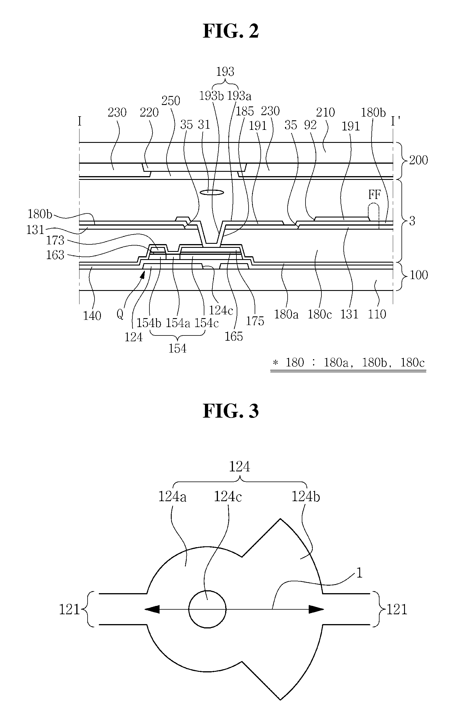
A thin film transistor array panel is capable of increasing an aperture ratio and decreasing parasitic capacitance between a gate electrode and a drain electrode by reducing an area of a thin film transistor. The thin film transistor array panel includes: a substrate; a gate line disposed on the substrate and including a gate electrode; a gate insulating layer on the gate line; a semiconductive island on the gate insulating layer; a circular drain electrode on the semiconductive island; and a source electrode disposed on the semiconductive island and shaped like a circular band bent in a direction from which the drain electrode is disposed. The gate electrode may include a circular portion that is overlapped by the drain electrode and a circular sector portion that is overlapped by the source electrode.

Description

CLAIM OF PRIORITY[0001]This application makes reference to, incorporates the same herein, and claims all benefits accruing under 35 U.S.C. §119 from an application earlier filed in the Korean Intellectual Property Office on the Oct. 1, 2014 and there duly assigned Serial No. 10-2014-0132356.BACKGROUND OF THE INVENTION[0002]1. Field of the Invention[0003]Embodiments of the inventive concept relate to a thin film transistor array panel capable of increasing an aperture ratio and decreasing parasitic capacitance between a gate electrode and a drain electrode by reducing an area of a thin film transistor.[0004]2. Description of the Related Art[0005]A liquid crystal display (LCD) includes a liquid crystal layer interposed between two transparent substrates and drives the liquid crystal layer so as to adjust transmittance for each pixel, and thus a desired color can be displayed.[0006]An LCD uses a variety of display modes in accordance with molecular arrangements in liquid crystals, and ...

Claims


Application Information

Patent Timeline
Patent Type & Authority Patents(United States)
IPC IPC(8): H01L27/00H01L29/00H01L29/423H01L27/12H01L29/417
CPCH01L29/42384H01L27/1222H01L29/41733H01L27/124
Inventor KWAK, YUN HEE
Owner SAMSUNG DISPLAY CO LTD
Learn More