
Resist pattern calculation method and calculation program storage medium

a technology of resist pattern and calculation method, which is applied in the direction of microlithography exposure apparatus, printers, instruments, etc., can solve the problems that resist pattern having a desired shape cannot be transferred onto the wafer in practice, and the device characteristics are deteriorated, so as to improve the calculation accuracy of resist pattern

Active Publication Date: 2016-09-20
CANON KK
View PDF6 Cites 1 Cited by
  • Summary
  • Abstract
  • Description
  • Claims
  • Application Information

AI Technical Summary

Benefits of technology

[0007]The present invention has been made in consideration of the above-mentioned situation, and provides a technique of improving the calculation accuracy of a resist pattern.

Problems solved by technology

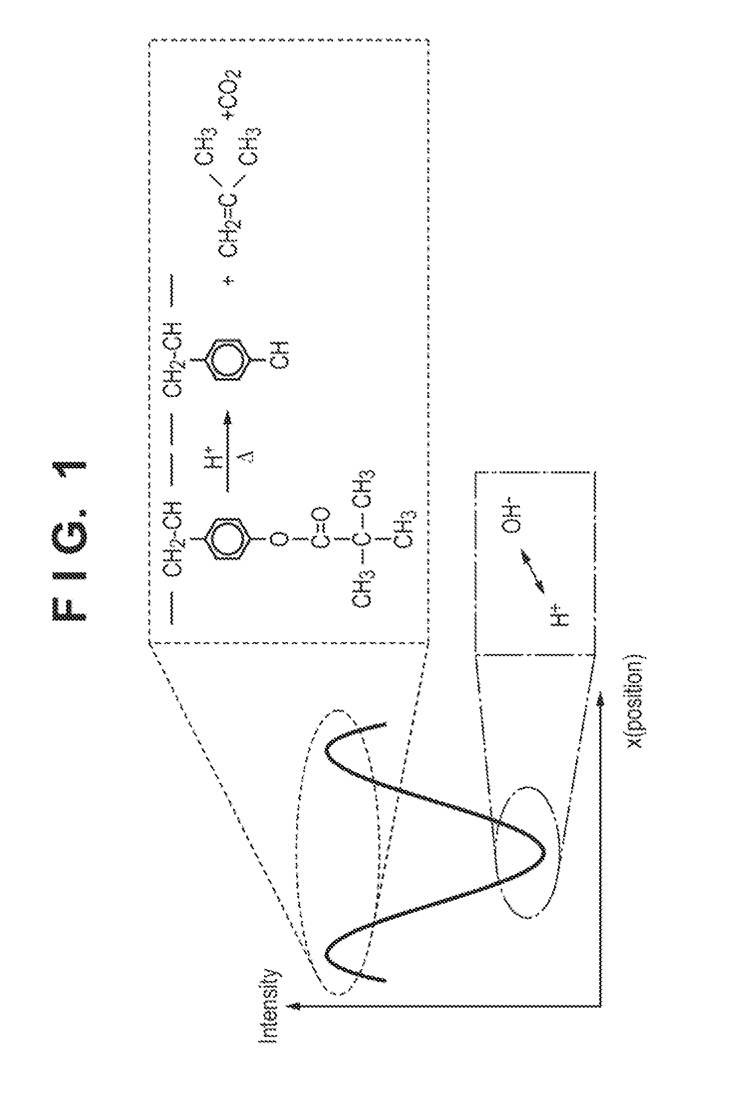
However, due to, for example, the optical proximity effect (OPE) and low k1, a resist pattern having a desired shape cannot be transferred onto the wafer in practice.
This is one factor which deteriorates the device characteristics.
Unfortunately, it is difficult for the prior art technique described in Japanese Patent Laid-Open No. 08-148404 to calculate the size of a resist pattern with high accuracy.

Method used


Image

  • Resist pattern calculation method and calculation program storage medium
  • Resist pattern calculation method and calculation program storage medium
  • Resist pattern calculation method and calculation program storage medium

Examples


example

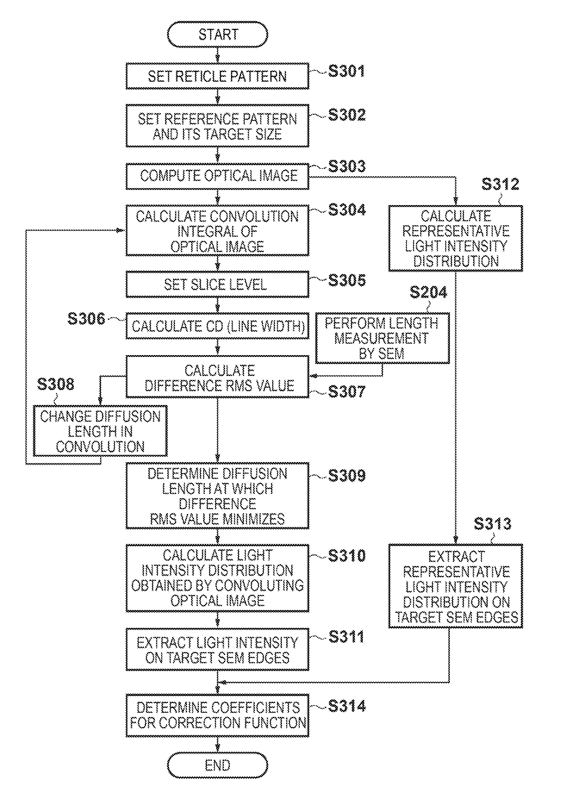
[0049]The Example in the above-described embodiment will be described. In step S301, a plurality of reticle patterns for use in modeling are set. FIG. 11 is a schematic view of patterns used. In pattern A, all bars have a length W=5 μm. Although pattern A has three lines in FIG. 11 for the sake of simplicity, it has 17 lines in practice. Also, pattern A has lines and spaces which are periodically arranged in the full field of pattern A, and the central line as an evaluation portion among the 17 lines. Twenty-five types of patterns A are obtained by defining different combinations of lines and space sizes. In pattern B, all bars have a length W=2 μm. Although pattern B has three lines in FIG. 11 for the sake of simplicity, it has nine lines in practice. Also, pattern B has lines, spaces, and gaps which are periodically arranged in the full field of pattern B, and the central line as an evaluation portion among the nine lines. Eight types of patterns B are obtained by defining differe...


PUM

PropertyMeasurementUnit
radiusaaaaaaaaaa
radiusaaaaaaaaaa
diffusion lengthaaaaaaaaaa

Abstract

A recording medium stores a program for causing a computer to execute a method of calculating a resist pattern. The method includes: a first step of calculating a light intensity distribution of an optical image formed on the resist, based on the reticle pattern and an exposure condition; a second step of convoluting, using a first diffusion length, the calculated light intensity distribution; a third step of calculating a representative light intensity from the calculated light intensity distribution or the convoluted light intensity distribution; a fourth step of correcting the convoluted light intensity distribution by adding, to the convoluted light intensity distribution, a correction function including a first function given by:{∑k=0n⁢(ak⁢Jk)}⁢exp⁡(-α⁢⁢J)where J is the distribution of the representative light intensity; and a fifth step of calculating the resist pattern based on the corrected light intensity distribution and a slice level set in advance.

Description

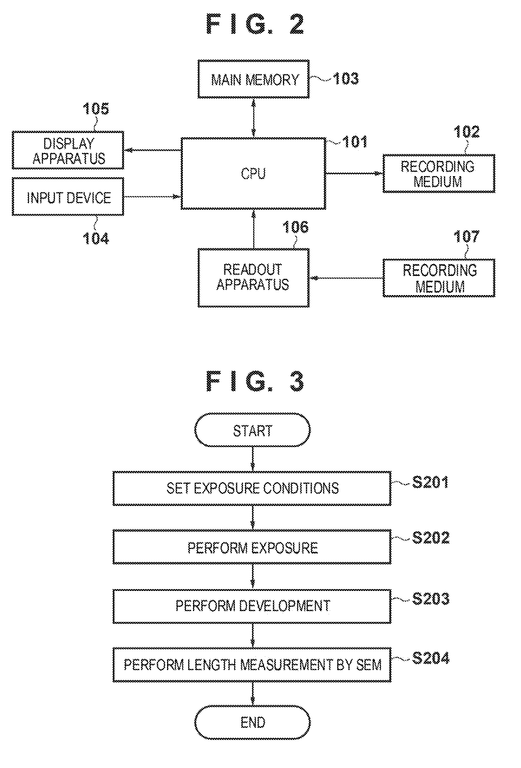
BACKGROUND OF THE INVENTION[0001]1. Field of the Invention[0002]The present invention relates to a resist pattern calculation method and a calculation program storage medium.[0003]2. Description of the Related Art[0004]In a lithography process, a resist pattern is formed by an exposure process in which light from a reticle pattern is projected onto a resist by a projection optical system to expose the resist to light, and a development process in which the exposed resist is developed. A resist pattern having a desired shape is desirably transferred and formed on the wafer. However, due to, for example, the optical proximity effect (OPE) and low k1, a resist pattern having a desired shape cannot be transferred onto the wafer in practice. This is one factor which deteriorates the device characteristics. Therefore, to improve the device characteristics, it is necessary to calculate the shape of a resist pattern.[0005]To calculate a resist pattern, Japanese Patent Laid-Open No. 08-14840...

Claims


Application Information

Patent Timeline
Patent Type & Authority Patents(United States)
IPC IPC(8): G03B27/32G03F7/20
CPCG03F7/705G03F7/70558G03F7/70608
Inventor NAKAYAMA, RYOTSUJITA, KOUICHIROUMIKAMI, KOJIISHII, HIROYUKI
Owner CANON KK
Learn More