Power semiconductor device

a technology of semiconductor devices and on-state losses, applied in the direction of semiconductor devices, electrical apparatus, transistors, etc., can solve the problems of negatively affecting igbt performance, and high igbt on-state losses, and achieve the effect of higher doping concentration

Active Publication Date: 2016-04-26
HITACHI ENERGY LTD
View PDF23 Cites 1 Cited by
  • Summary
  • Abstract
  • Description
  • Claims
  • Application Information

AI Technical Summary

Benefits of technology

[0040]The well brings improvements in the diode mode because the influence of the MOS channel during the forward conduction of the diode is reduced and the voltage snap-back at low currents when the gate emitter voltage above the threshold on the gate is applied is also reduced. The influence of the gate control on the diode is reduced by the exemplary arrangements described herein.
[0041]By the introduction of the well, an additional diode emitter area is introduced, which is decoupled from the MOS channel. The well is placed outside of the active IGBT cell in such a way that it is not located between the cells in the PIN diode region, and therefore does not affect the performance of the device in the IGBT mode and does not influence the cell design parameters (e.g. pitch). As a result, the well does not incorporate MOS control. The well or well zones can have different doping, depth, and lifetime killing scheme from that of the base layer. The well can be designed to be partially floating (by contacting the well to emitter electrode via the base layer) or non-floating (the well directly contacting the emitter electrode) depending on the optimum injection from the additional p-well region desired.

Problems solved by technology

By applying a gate voltage above the threshold, the plasma is extracted through the induced channel, therefore reducing the plasma below the p-type base layer 4, which results in higher on-state losses compared to the situation when the gate emitter voltage is below the threshold level or negative.
This alternating arrangement, however, negatively influences the IGBT performance.
This device also suffers from the p-layers being arranged in the same direction as the base layers (in a line with the base layers) and from the large contact area of the anode layer to the emitter electrode, from which high IGBT on-state losses result.
Therefore, this device has the same disadvantages as mentioned above.

Method used


Image

  • Power semiconductor device
  • Power semiconductor device
  • Power semiconductor device

Examples


Embodiment Construction

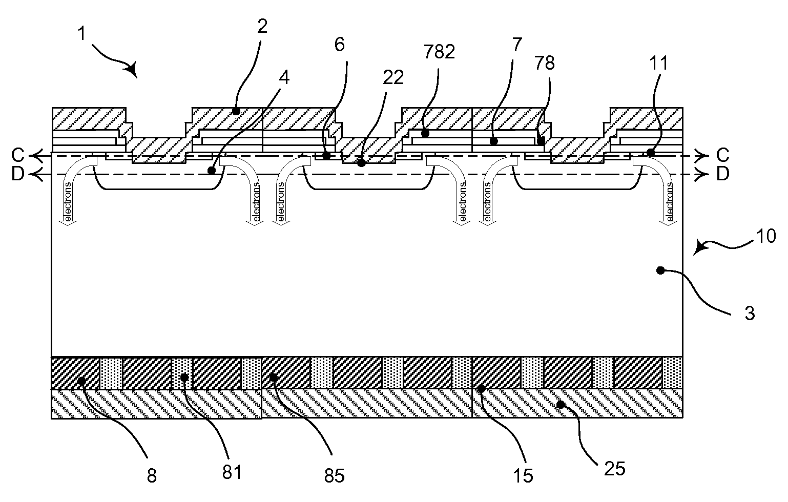
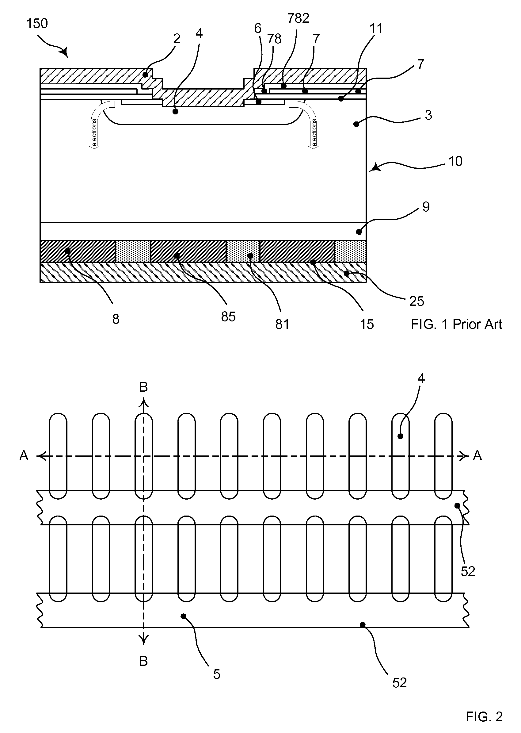
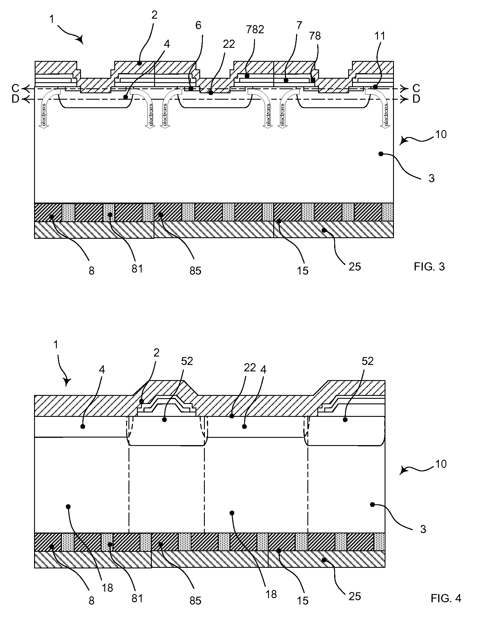
[0035]Exemplary embodiments of the present disclosure provide a reverse conducting power semiconductor device with improved performance of the device in diode mode.

[0036]An exemplary power semiconductor device includes layers of different conductivity types in a wafer, which layers are arranged between an emitter electrode on an emitter side and a collector electrode on a collector side, which is arranged opposite of the emitter side.

[0037]The device includes the following layers a drift layer of a first conductivity type, which is arranged between the emitter side and the collector side, a first layer, which includes a first region of the first conductivity type and higher doping concentration than the drift layer and a second region of a second conductivity type, which is different from the first conductivity type, which second region is arranged adjacent to the first region, wherein the first layer is arranged between the drift layer and the collector electrode, a base layer of a...


PUM


Abstract

An exemplary power semiconductor device with a wafer having an emitter electrode on an emitter side and a collector electrode on a collector side, an (n-) doped drift layer, an n-doped first region, a p-doped base layer, an n-doped source region, and a gate electrode, all of which being formed between the emitter and collector electrodes. The emitter electrode contacts the base layer and the source region within a contact area. An active semiconductor cell is formed within the wafer, and includes layers that lie in orthogonal projection with respect to the emitter side of the contact area of the emitter electrode. The device also includes a p-doped well, which is arranged in the same plane as the base layer, but outside the active cell. The well is electrically connected to the emitter electrode at least one of directly or via the base layer.

Description

RELATED APPLICATIONS[0001]This application is a continuation under 35 U.S.C. §120 of International Application PCT / EP2011 / 060089 filed on Jun. 17, 2011, designating the U.S. and claiming priority to European application EP 10166258.3 filed in Europe on Jun. 17, 2010, the contents of which are hereby incorporated by reference in their entireties.FIELD[0002]The disclosure relates to power semiconductor devices, such as a power semiconductor device with layers of different conductivity types.BACKGROUND INFORMATION[0003]FIG. 1 shows a reverse-conducting insulated gate bipolar transistor (RC-IGBT) with a planar gate electrode according to a known implementation. As shown in FIG. 1, the RC-IGBT includes within one wafer 10 an insulated gate bipolar transistor with a built-in freewheeling diode. Such a reverse-conducting semiconductor device 150 includes an n-type drift layer 3 with a first main side, which is the emitter side 11 of the integrated IGBT, and a second main side, which is the...

Claims


Application Information

Patent Timeline
Patent Type & Authority Patents(United States)
IPC IPC(8): H01L27/088H01L29/06H01L29/10H01L29/739
CPCH01L29/0696H01L29/1095H01L29/7395H01L29/7396H01L27/088
Inventor STORASTA, LIUTAURASKOPTA, ARNOSTRAHIMO, MUNAF
Owner HITACHI ENERGY LTD
Why Eureka
Try Eureka