
Single- layer full-mesh, point-to-point network

a point-to-point network and single-layer technology, applied in the direction of instruments, optical waveguide light guides, optics, etc., can solve the problems of large link-loss budget, large number of optical waveguide crossings, and obstacle to the use of this technology

Active Publication Date: 2016-04-19
ORACLE INT CORP
View PDF7 Cites 7 Cited by
  • Summary
  • Abstract
  • Description
  • Claims
  • Application Information

AI Technical Summary

Benefits of technology

The patent text describes a multi-chip module (MCM) with a single optical routing layer that connects multiple chip components through optical waveguides without the need for cross-talk. The network includes a cyclic de-multiplexer that separates optical signals and directs them to the proper chip. The module has a substrate and a semiconductor layer, and uses a variety of optical signals and full-mesh point-to-point connectivity. The technical effects of this invention include increased speed, reliability, and reduced latency in communication among different chip components, leading to improved performance and efficiency.

Problems solved by technology

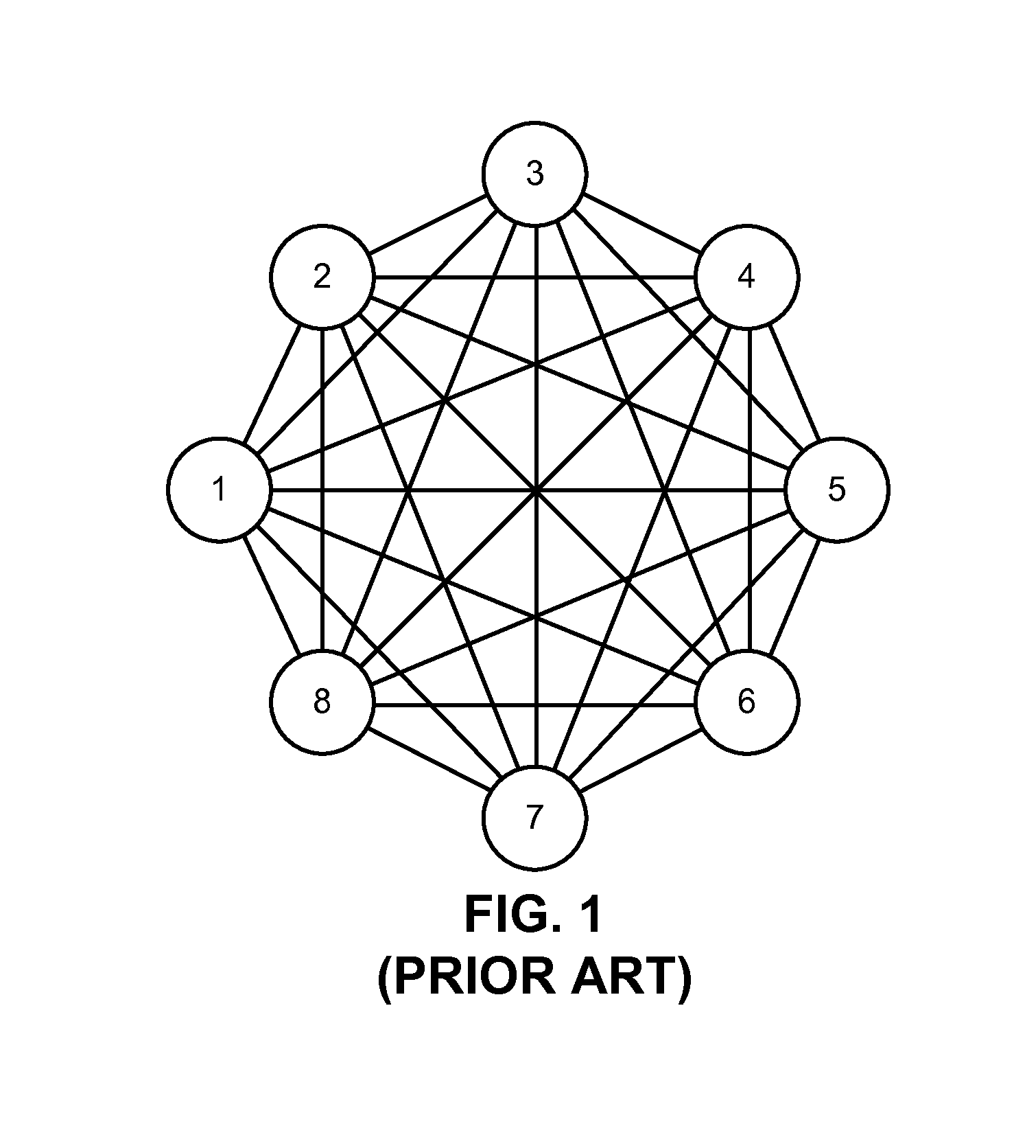
However, implementing such a fully connected mesh network using silicon optical waveguides on a silicon-on-insulator (SOI) substrate may involve a large number of optical-waveguide crossings.
Even though special crossing designs manage to reduce the channel loss and crosstalk significantly (less than 0.1 dB insertion loss and less than −40 dB crosstalk), the hundreds of optical-waveguide crossings in an MCM would still significantly impact performance and, therefore, could pose an obstacle to the use of this technology.
As a consequence, currently four OPxC hops will add a total of 12 dB to the link loss, which results in large link-loss budget and significantly limits the energy efficiency of the WDM links and the interconnect network as a whole.
While there are ongoing improvements in OPxCs, the losses associated with OPxC hops are expected to remain significant.

Method used


Image

  • Single- layer full-mesh, point-to-point network
  • Single- layer full-mesh, point-to-point network
  • Single- layer full-mesh, point-to-point network

Examples


Embodiment Construction

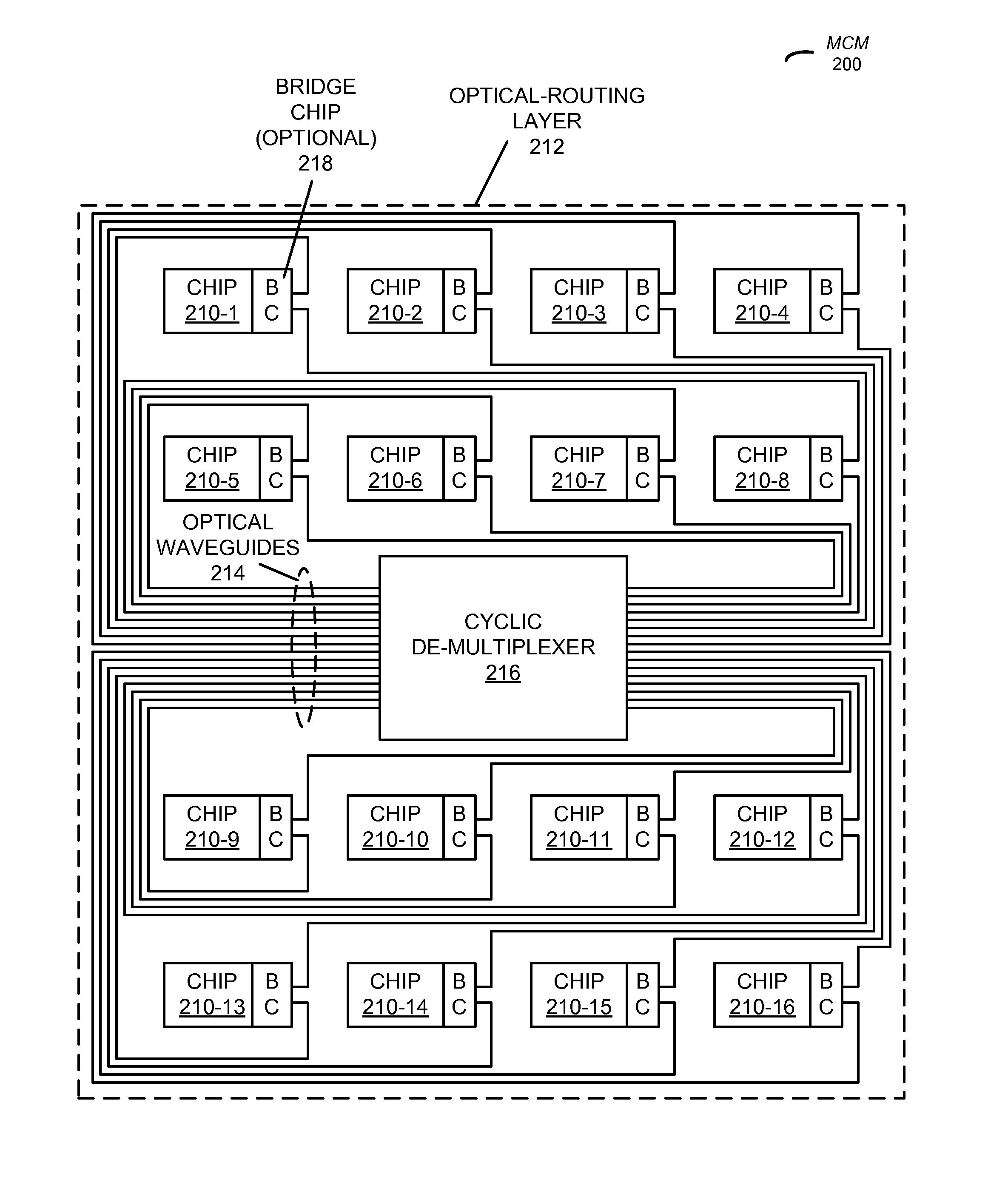
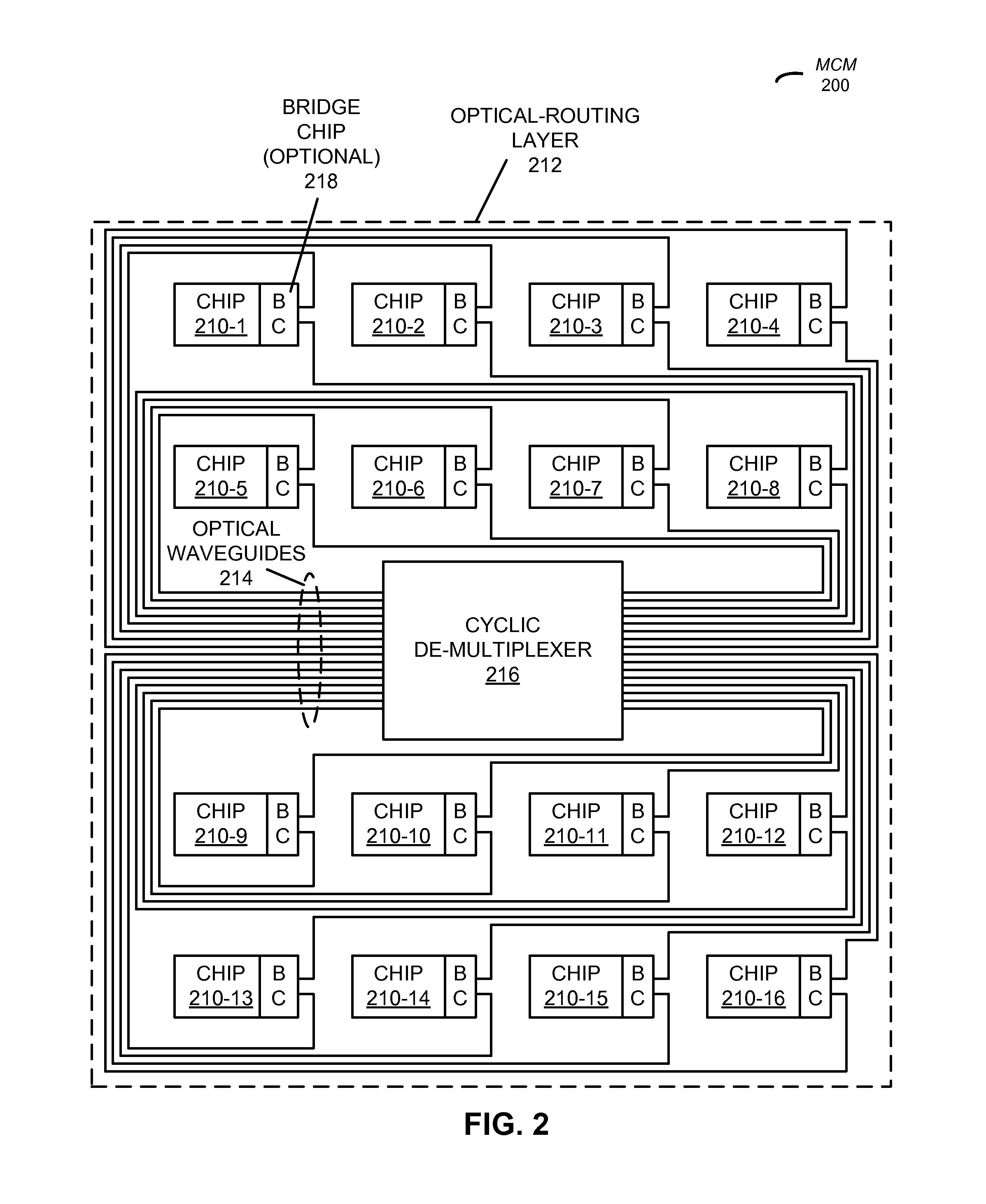
[0027]Embodiments of a multi-chip module (MCM), a system that includes the MCM, and a method for communicating among N chips in the MCM are described. This MCM may include a single optical routing layer that provides point-to-point connectivity among N chips in the MCM, such as all-to-all connectivity or full-mesh point-to-point connectivity. Moreover, the optical routing layer may include: N optical waveguides optically coupled to the N chips; and a cyclic de-multiplexer, optically coupled to the N optical waveguides, that routes optical signals among the N optical waveguides without optical waveguide crossing in the optical routing layer. For example, the cyclic de-multiplexer may include: an array-waveguide-grating (AWG) wavelength router and / or an echelle-grating wavelength router.

[0028]By interconnecting the N chips using the single optical routing layer, the MCM may not need non-blocking dedicated optical channels among the N chips, and may avoid optical-waveguide crossings an...


PUM


Abstract

An MCM may include a single optical routing layer that provides point-to-point connectivity among N chips in the MCM, such as all-to-all connectivity or full-mesh point-to-point connectivity. Moreover, the optical routing layer may include: N optical waveguides optically coupled to the N chips and a cyclic de-multiplexer, optically coupled to the N optical waveguides, that routes optical signals among the N optical waveguides without optical-waveguide crossing in the optical routing layer. For example, the cyclic de-multiplexer may include: an array-waveguide-grating (AWG) wavelength router and / or an echelle-grating wavelength router.

Description

GOVERNMENT LICENSE RIGHTS[0001]This invention was made with United States Government support under Agreement No. HR0011-08-9-0001 awarded by DARPA. The United States Government has certain rights in the invention.BACKGROUND[0002]1. Field[0003]The present disclosure generally relates to the design of multi-chip modules (MCMs). More specifically, the present disclosure relates to the design of an MCM that includes a cyclic de-multiplexer in a single optical routing layer that provides full-mesh, point-to-point connectivity among chips in the MCM.[0004]2. Related Art[0005]Engineers are researching a multi-chip module (MCM) that integrates multiple silicon chips together into a logically contiguous piece of silicon larger than a single reticle using high-speed interconnects, such as silicon-photonic wavelength-division-multiplexing (WDM) interconnects. In order to intimately interconnect chip sites within the MCM with low latency and high bandwidth without blocking, a full-mesh, point-t...

Claims


Application Information

Patent Timeline
Patent Type & Authority Patents(United States)
IPC IPC(8): G02B6/12G02B6/34G02B6/28G02B6/42G02B6/293G02B6/43
CPCG02B6/12009G02B6/29326G02B6/29328G02B6/43G02B6/2938G02B2006/12107
Inventor KRISHNAMOORTHY, ASHOK V.ZHENG, XUEZHE
Owner ORACLE INT CORP
Learn More