Camera module including conductive layer corresponding to shape of electronic circuit pattern layer

a technology of electronic circuit pattern and camera module, which is applied in the field of camera module, can solve the problems of increasing the size of the camera module, and achieve the effects of reducing processing costs, reducing manufacturing difficulty, and manufacturing at a more reasonable pri

Active Publication Date: 2016-02-23
LG INNOTEK CO LTD
View PDF14 Cites 2 Cited by
  • Summary
  • Abstract
  • Description
  • Claims
  • Application Information

AI Technical Summary

Benefits of technology

[0027]The camera module according to the present invention has an advantageous effect in that an electronic circuit can be formed on a surface of an injection-molded electronic component in the same method as that of formation of an electronic circuit pattern layer on the surface of the electronic component to form a circuit on a PCB, whereby the electronic components can be manufactured at a more reasonable price.
[0028]Another advantage is that a reduced difficulty in manufacturing process enables manufacturing of a product with a constant level of reliability regardless of skill of an operator, whereby a processing cost can be reduced.

Problems solved by technology

However, in a case the connection substrate is separately provide as mentioned above, there is a problem in manufacturing the connection substrate and managing stock control.
Another problem is that size of the camera module increases as much as volume of the connection substrate.

Method used


Image

  • Camera module including conductive layer corresponding to shape of electronic circuit pattern layer
  • Camera module including conductive layer corresponding to shape of electronic circuit pattern layer

Examples


Embodiment Construction

[0032]The following description is not intended to limit the invention to the form disclosed herein. Consequently, variations and modifications commensurate with the following teachings, and skill and knowledge of the relevant art are within the scope of the present invention. The embodiments described herein are further intended to explain modes known of practicing the invention and to enable others skilled in the art to utilize the invention in such, or other embodiments and with various modifications required by the particular application(s) or use(s) of the present invention.

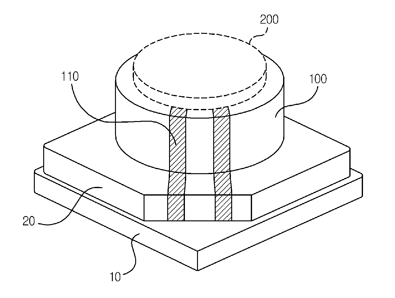
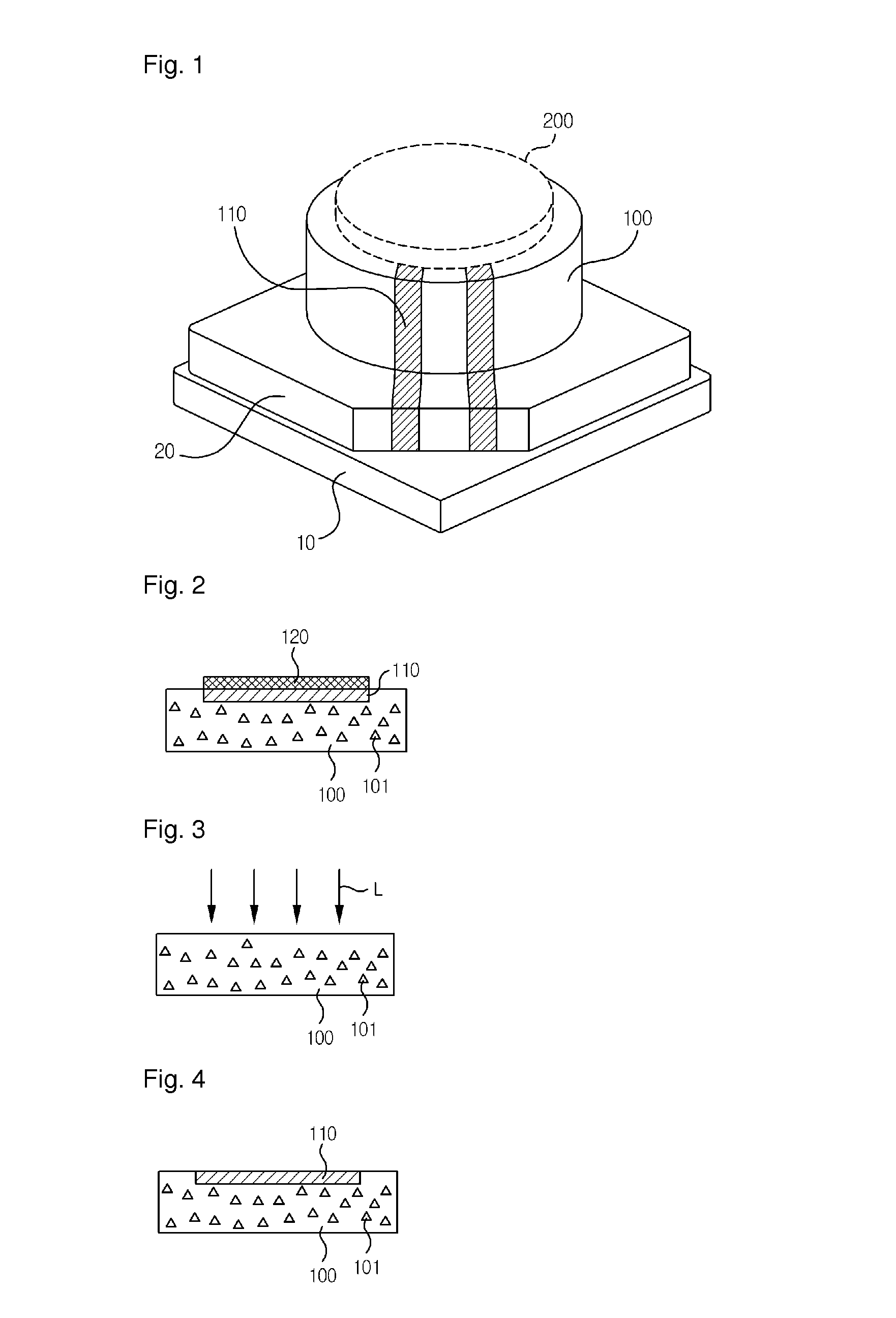
[0033]The disclosed embodiments and advantages thereof are best understood by referring to FIGS. 1-4 of the drawings, like numerals being used for like and corresponding parts of the various drawings. Other features and advantages of the disclosed embodiments will be or will become apparent to one of ordinary skill in the art upon examination of the following figures and detailed description. It is intended ...


PUM


Abstract

The present invention relates to a camera module, the camera module including a PCB (Printed Circuit Board) formed with an image sensor, a holder formed at an upper surface of the PCB and mounted therein with at least one or more lenses, an actuator positioned at the holder, and an electronic circuit pattern layer formed on the holder.

Description

TECHNICAL FIELD[0001]The present invention relates to a camera module.BACKGROUND ART[0002]A PCB (Printed Circuit Board) is a component connecting an electric circuit between electronic components to supply a power and a control signal. Recently, a camera module performing an auto focusing operation using an actuator has been developed, where two electrodes of an AF (Auto Focus) terminal and a PCB AF pad are conductively connected to controllably drive the actuator.[0003]The actuator needs to receive a control signal and a power by connecting the PCB mounted with an image sensor, and to this end, a separate connection substrate functioning as a wiring is generally provided between the actuator and the PCB. However, in a case the connection substrate is separately provide as mentioned above, there is a problem in manufacturing the connection substrate and managing stock control. Another problem is that size of the camera module increases as much as volume of the connection substrate.D...

Claims


Application Information

Patent Timeline
Patent Type & Authority Patents(United States)
IPC IPC(8): H04N5/225H05K1/18H04N5/228H05K1/14
CPCH04N5/2253H04N5/2257H05K1/181H05K1/141H05K2201/049H05K2201/10151Y02P70/50H04N23/57G03B13/36H04N23/54
Inventor HAN, KWANGJOON
Owner LG INNOTEK CO LTD
Why Eureka
Try Eureka