Semiconductor device having chip embedded in heat spreader and electrically connected to interposer and method of manufacturing the same

a technology of semiconductor devices and heat spreaders, which is applied in the direction of semiconductor devices, semiconductor/solid-state device details, electrical apparatus, etc., can solve the problems of significant thermal, electrical and reliability challenges in the semiconductor packaging industry, performance degradation problems, and shorting between neighboring neighbors, so as to achieve sufficient mechanical rigidity and improve production yield

Inactive Publication Date: 2016-01-05
BRIDGE SEMICON
View PDF8 Cites 0 Cited by
  • Summary
  • Abstract
  • Description
  • Claims
  • Application Information

AI Technical Summary

Benefits of technology

[0006]A primary objective of the present invention is to provide a semiconductor device in which a chip-on-interposer subassembly is configured wherein a chip is assembled to an interposer by a plurality of bumps so as to avoid laser or photo-imaging process directly acting on chip I / O pads, thereby improving the production yield and reliability of the semiconductor device.
[0007]Another objective of the present invention is to provide a semiconductor device in which an interposer is used to provide fan-out routing for the chip attached thereon. As the chip is electrically connected to one side of the interposer for fan-out through the interposer, a buildup circuitry can be connected to another side of the interposer with much larger contact pad pitch, thereby resolving chip I / O pad crowding problem and improving the production yield and reliability of the semiconductor device.
[0008]Yet another objective of the present invention is to provide a semiconductor device in which a chip is enclosed in a cavity of a heat spreader so as to effectively dissipate the heat generated by the chip, thereby improving signal integrity and electrical performance of the semiconductor device.
[0009]In accordance with the foregoing and other objectives, the present invention proposes a semiconductor device that includes a chip, an interposer, a heat spreader, an encapsulant and a buildup circuitry. The interposer, interconnected to the chip by bumps, provides primary fan-out routing for the chip so that the possible bond pad disconnection induced by tight I / O pad pitch can be avoided. The heat spreader, having a cavity, is thermally conductible to the chip by a thermally conductive material to provide thermal dissipation for the chip positioned in the cavity. The buildup circuitry, adjacent to the encapsulant and the interposer and electrically connected to the interposer, provides secondary fan-out routing for the chip and has a patterned array of terminal pads that matches the next level assembly wiring board.
[0013]The method of making a semiconductor device according to the present invention has numerous advantages. For instance, forming the chip-on-interposer subassembly before attaching it to the heat spreader can ensure the chip is electrically connected so that any contact pad disconnection problem inherent to micro-via process can be avoided. Using the semi-finished interposer to interconnect the chip can avoid the need of creating metallized through vias in the interposer before it is integrated into a 2.5D substrate, thereby resolving through via metal plating problem and improving the production yield. Additionally, as interposer grinding is executed after providing the encapsulant and the heat spreader to support the interposer, it can provide sufficient mechanical rigidity for the ground interposer. Moreover, the two-step forming of the interconnect substrate for the chip is beneficial as the interposer can provide primary fan-out routing whereas the buildup circuitry provide further fan-out routing and horizontal interconnections between the upper and the lower devices.

Problems solved by technology

The convergence of mobility, communication, and computing has created significant thermal, electrical and reliability challenges to the semiconductor packaging industry.
Despite numerous configurations for embedding semiconductor chip in wiring board or mold compound reported in the literature, many manufacturing and performance-related deficiencies remain.
However, these disclosed devices may render performance degradation problems as the heat generated by the embedded chip can't be dissipated properly through the thermally insulating material such as laminate or mold compound.
As a result, the use of the micro-via approach presents a crowding problem which can cause shorting between the neighboring micro-vias.
Another significant drawback arising from the fabrication of the above devices is that the embedded chip may dislocate during encapsulation or lamination.
Incomplete metallization of micro-vias due to chip dislocation as described in U.S. Pat. No. 8,501,544 further degrades the quality of the electrical connection, thereby lowering the reliability and production yield of the fabricated device.

Method used


Image

  • Semiconductor device having chip embedded in heat spreader and electrically connected to interposer and method of manufacturing the same
  • Semiconductor device having chip embedded in heat spreader and electrically connected to interposer and method of manufacturing the same
  • Semiconductor device having chip embedded in heat spreader and electrically connected to interposer and method of manufacturing the same

Examples


Embodiment Construction

[0035]Hereafter, an example will be provided to illustrate the embodiment of the present invention. Advantages and effects of the invention will become more apparent from the disclosure of the present invention. It should be noted that these accompanying figures are simplified and illustrative. The quantity, shape and size of components shown in the figures may be modified according to practical conditions, and the arrangement of components may be more complex. Other various aspects also may be practiced or applied in the invention, and various modifications and variations can be made without departing from the spirit of the invention based on various concepts and applications.

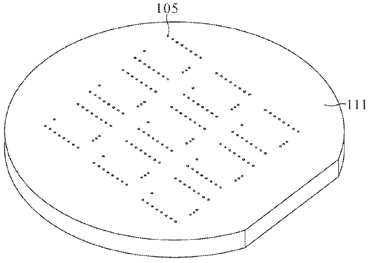
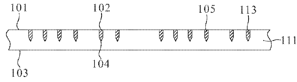
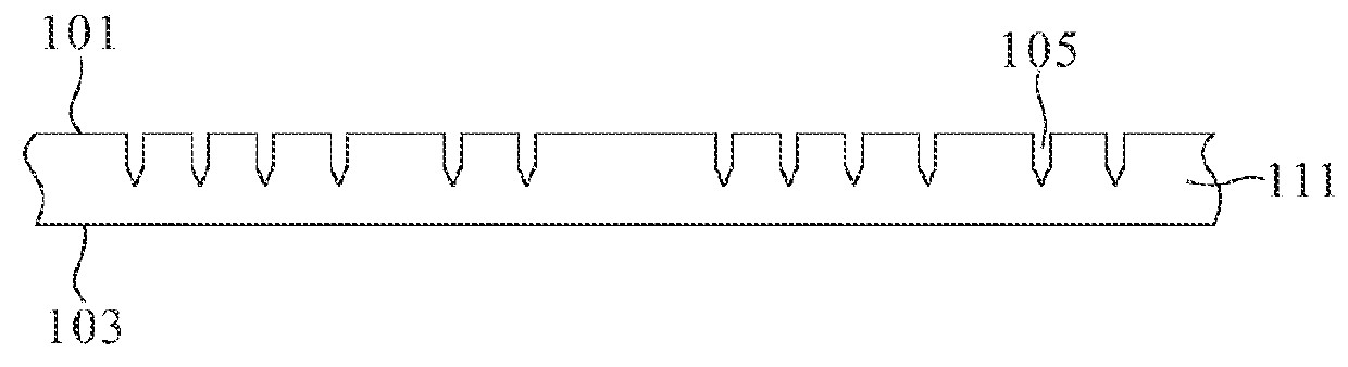
[0036]FIGS. 1-25 are schematic views showing a method of making a semiconductor device, which includes an interposer, a chip, a heat spreader, an encapsulant and a buildup circuitry in accordance with an embodiment of the present invention.

[0037]As shown in FIG. 25, the semiconductor device 100 includes an int...


PUM


Abstract

A method of making a semiconductor device is characterized by the step of attaching a chip-on-interposer subassembly to a heat spreader with the chip inserted into a cavity of the heat spreader and the interposer laterally extending beyond the cavity. The interposer backside process is executed after the chip-on-interposer attachment and encapsulation to form the finished interposer. The heat spreader provides thermal dissipation, and the finished interposer provides primary fan-out routing for the chip. In the method, a buildup circuitry is electrically coupled to the interposer to provide further fan-out routing.

Description

CROSS REFERENCE TO RELATED APPLICATION[0001]This application claims the benefit of filing date of U.S. Provisional Application Ser. No. 61 / 941,656 filed Feb. 19, 2014. The entirety of said Provisional Application is incorporated herein by reference.FIELD OF THE INVENTION[0002]The present invention relates to a semiconductor device, and more particularly to a semiconductor device having a chip embedded in a heat spreader and electrically connected to an interposer, and to a method of making the same.DESCRIPTION OF RELATED ART[0003]The convergence of mobility, communication, and computing has created significant thermal, electrical and reliability challenges to the semiconductor packaging industry. Despite numerous configurations for embedding semiconductor chip in wiring board or mold compound reported in the literature, many manufacturing and performance-related deficiencies remain. For example, U.S. Pat. Nos. 8,742,589, 8,735,222, 8,679,963 and 8,453,323 disclose semiconductor devi...

Claims


Application Information

Patent Timeline
Patent Type & Authority Patents(United States)
IPC IPC(8): H01L21/44H01L23/00H01L23/498H01L21/48H01L21/50H01L21/56H01L23/31H01L23/367H01L21/768
CPCH01L23/49827H01L21/486H01L21/4825H01L21/4871H01L21/563H01L21/76895H01L23/3157H01L23/3675H01L23/49811H01L24/17H01L24/81H01L2224/16113H01L2224/16235H01L2924/12042H01L2924/181H01L2924/351H01L2924/00H01L21/4853H01L21/4882H01L23/367H01L23/49838H01L21/561H01L23/142H01L23/3121H01L23/5389H01L23/552H01L24/97H01L2224/0401H01L2224/13023H01L2224/13139H01L2224/13144H01L2224/13147H01L2224/32225H01L2224/32245H01L2224/73204H01L2224/73253H01L2224/81203H01L2224/81207H01L2224/81815H01L2224/92125H01L2224/92225H01L2224/97H01L2924/15311H01L2924/15313H01L2924/16235H01L2924/16251H01L2224/83H01L2224/81H01L2924/00014H01L2224/16225
Inventor LIN, CHARLES W. C.WANG, CHIA-CHUNG
Owner BRIDGE SEMICON
Why Eureka
Try Eureka