
Pixel array and liquid crystal display device

a liquid crystal display and pixel array technology, applied in semiconductor devices, optics, instruments, etc., can solve the problem of interlaced flicker in the pixel array, and achieve the effect of simplifying the process for forming the pixel array, reducing cost and simplifying the process flow

Active Publication Date: 2015-11-03
SHANGHAI AVIC OPTOELECTRONICS +1
View PDF3 Cites 0 Cited by
  • Summary
  • Abstract
  • Description
  • Claims
  • Application Information

AI Technical Summary

Benefits of technology

The technical solution of this patent has the advantage of arranging transistors in the pixel units in the same direction, which ensures consistent feed-through voltage and prevents flicker in the pixel units. Additionally, the process for forming the pixel array is simpler, resulting in lower cost. The invention also allows for the achievement of dot inversion using data signals with opposite polarities, while reducing power consumption and simplifying the data signals required.

Problems solved by technology

However, the problem of interlaced flicker exists in the pixel array in the prior art when displaying pictures.

Method used


Image

  • Pixel array and liquid crystal display device
  • Pixel array and liquid crystal display device
  • Pixel array and liquid crystal display device

Examples


second embodiment

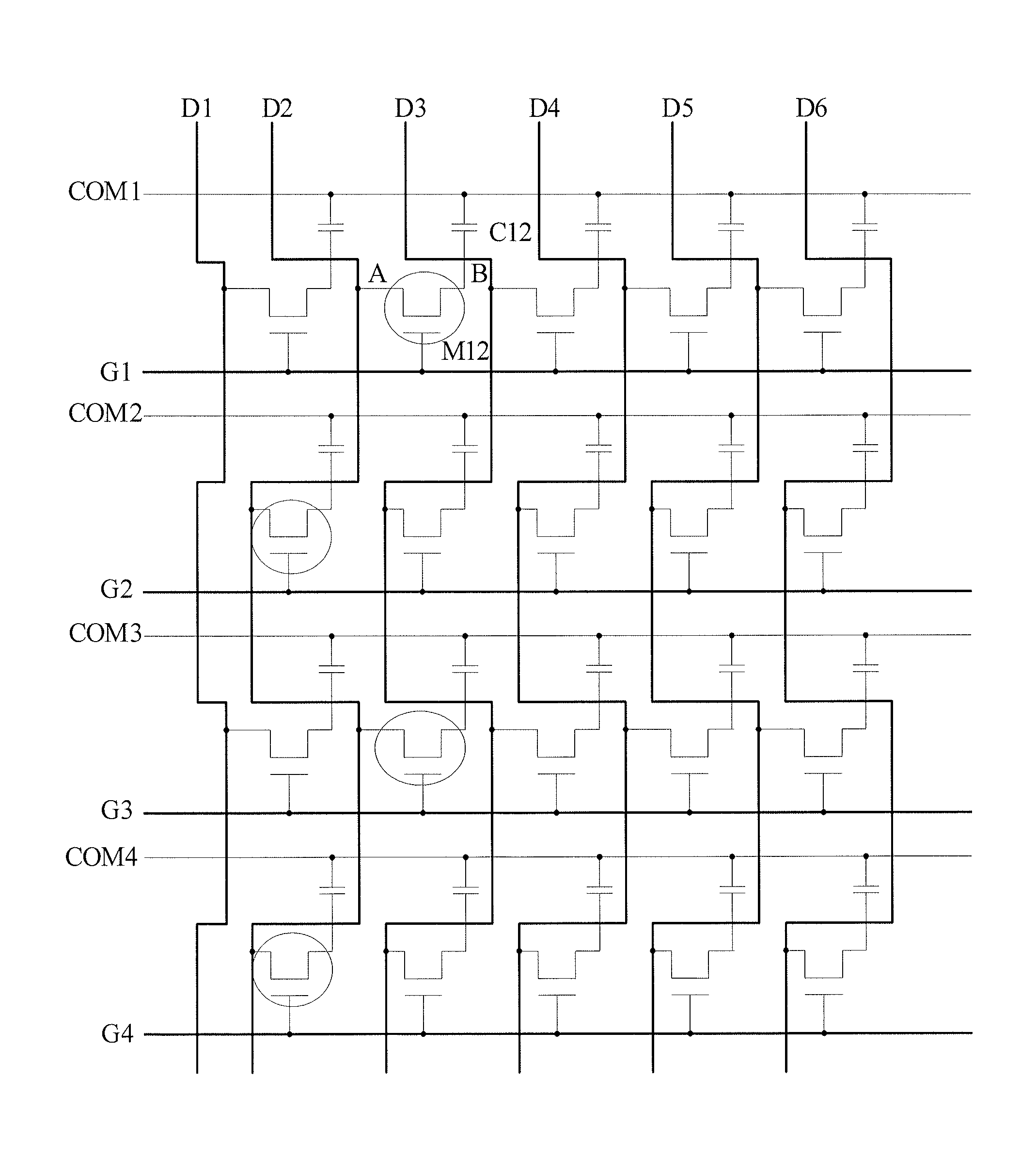
[0078]FIG. 12 is an equivalent schematic diagram showing a pixel array according to the invention. As shown in FIG. 12, the pixel array according to this embodiment includes: pixel units, data lines quantitatively corresponding to the number of columns N of the pixel units, and scan lines quantitatively corresponding to the number of rows of the pixel units, wherein[0079]transistors in the pixel units are arranged in the same direction;[0080]the pixel units in a same row are connected to a same scan line;[0081]the pixel units in each column and in odd rows are connected respectively to corresponding one of the data lines;[0082]the pixel units in each column and in even rows are connected respectively to corresponding one of the data lines; and[0083]the pixel units in the nth column and in even rows and the pixel units in the (n−1)th column and in odd rows are connected to a same data line, where n=2, . . . , N.

[0084]The pixel array in this embodiment differs from that in the embodim...

first embodiment

[0087]In addition, the pixel array 100 may have either the pixel array structure or the pixel array structure according to the embodiment shown in FIG. 12. As for the specific structures, reference may be made to the description about FIG. 7 and FIG. 11, which is not described here.

[0088]The scan drive circuit 200 is connected to the scan lines of the pixel array 100 and adapted to provide corresponding scan signals SG1 to SG4 to the scan lines, and the data drive circuit 300 is connected to the data lines of the pixel array 100 and adapted to provide corresponding data signals SD1 to SD6 to the data lines.

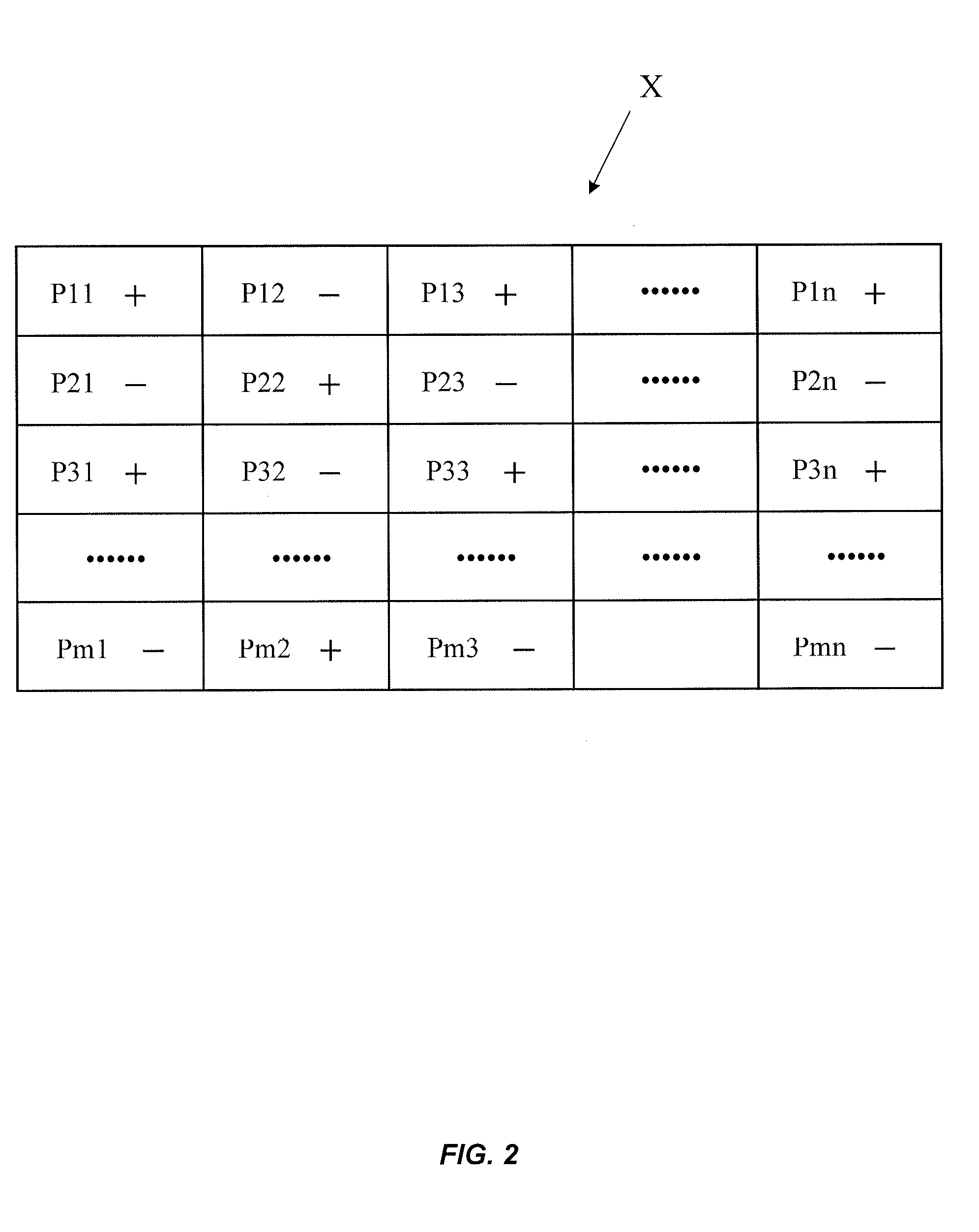
[0089]In the liquid crystal display device according to this embodiment, the data drive circuit 300 is adapted to provide data signals with opposite polarities to two adjacent data lines in the same frame, and adapted to provide data signals with opposite polarities to the same data line in two adjacent frames.

[0090]For example, in a first frame, the polarity of the data signal S...


PUM

PropertyMeasurementUnit
widthaaaaaaaaaa
widthaaaaaaaaaa
channel lengthaaaaaaaaaa

Abstract

A pixel array includes: pixel units, data lines quantitatively corresponding to the number of columns N of the pixel units, and scan lines quantitatively corresponding to the number of rows of the pixel units, wherein transistors in the pixel units are arranged in the same direction; the pixel units in the same row are connected to the same scan line; the pixel units in each column and in odd rows are connected respectively to corresponding one of the data lines; the pixel units in each column and in even rows are connected respectively to corresponding one of the data lines; and the pixel units in the nth column and in even rows and the pixel units in the n+1 th column and in odd rows are connected to the same data line, where n=1, 2, . . . , N.

Description

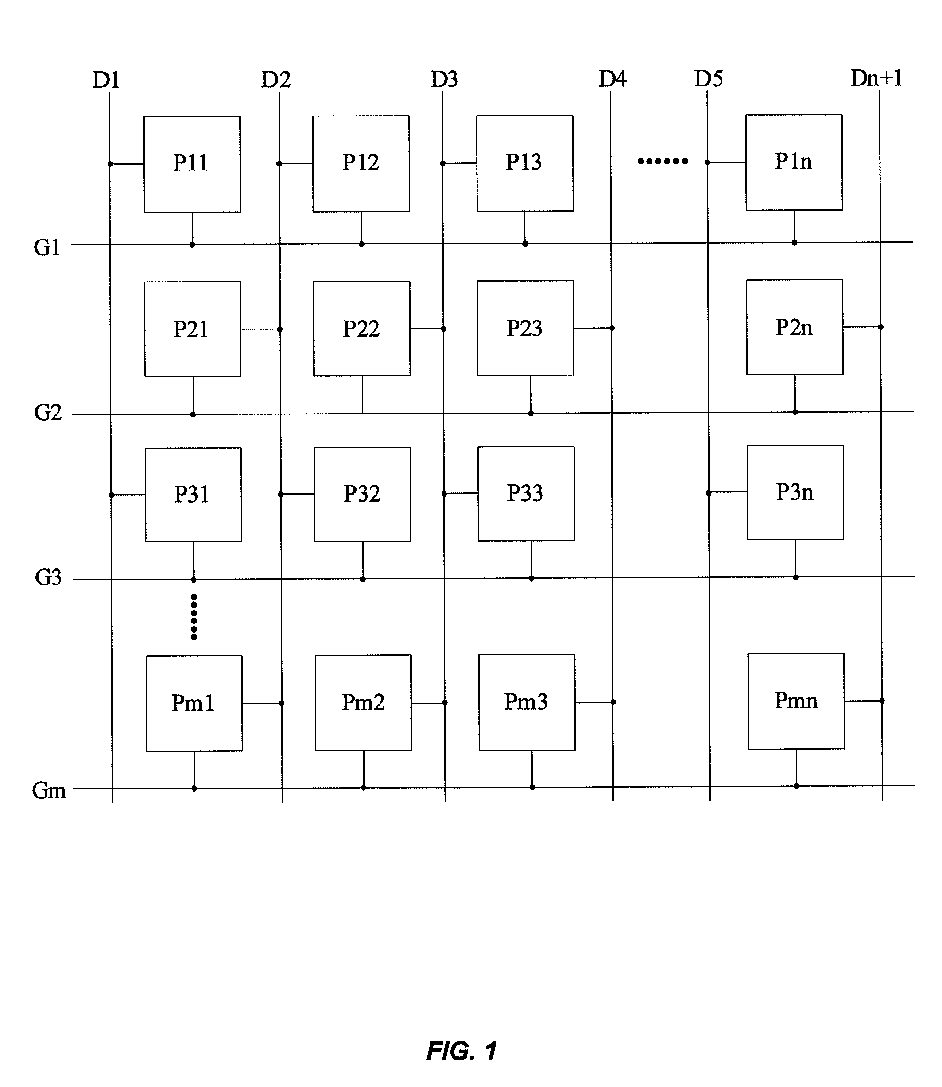
CROSS-REFERENCES TO RELATED APPLICATIONS[0001]This application claims the benefit of priority to Chinese Patent Application No. 201310342941.9, filed with the Chinese Patent Office on Aug. 7, 2013 and entitled “PIXEL ARRAY AND LIQUID CRYSTAL DISPLAY DEVICE”, the content of which is incorporated herein by reference in its entirety.TECHNICAL FIELD[0002]The present invention relates to the field of liquid crystal display, and particularly to a pixel array and a liquid crystal display device.BACKGROUND OF THE INVENTION[0003]With the development of technology, liquid crystal display device has become one of the most widely used flat panel display devices. An existing liquid crystal display device generally includes a scan drive circuit, a data drive circuit and a pixel array. FIG. 1 is a schematic diagram showing an existing pixel array. As shown in FIG. 1, the pixel array includes: a plurality of scan lines G1 to Gm, a plurality of data lines D1 to D(n+1), and a plurality of pixel units...

Claims


Application Information

Patent Timeline
Patent Type & Authority Patents(United States)
IPC IPC(8): G02F1/1337G02F1/1362G02F1/1368G09G3/36G02F1/1343H01L27/12
CPCG02F1/134336G02F1/1368G02F1/133707G02F1/136286G09G3/3648H01L27/1255G09G3/3614G09G2300/0426
Inventor XU, XINXIA, ZHIQIANGDUN, DONGLIANG
Owner SHANGHAI AVIC OPTOELECTRONICS
Learn More