Micro electronic component structure

a technology of electronic components and components, applied in the direction of emergency connections, sustainable manufacturing/processing, final product manufacturing, etc., can solve the problems of poor electrical contact, more materials, complex manufacturing process, etc., to prolong the life span of electronic components, avoid elastic fatigue, and improve the stability of electrical connections

Active Publication Date: 2015-10-13
KING YUAN ELECTRONICS
View PDF2 Cites 0 Cited by
  • Summary
  • Abstract
  • Description
  • Claims
  • Application Information

AI Technical Summary

Benefits of technology

[0008]One objective of the invention is to provide a micro electronic component structure with a simple structure, easy manufacture, and a high reliability.
[0020]In the invention, the electronic component structure of composite multi-factor deformation characteristics is formed by the micro terminal made of an elastic material and the bonding material with an elastic effect. The terminal without pins is used to avoid elastic fatigue and deformation under long-time operation due to the single elastic coefficient. Further, since the bonding material forms a sealed cyclic structure and the internal gas is compressed, the deformed structure is supported in a vapor-pressure type additionally, thus prolonging the life span of the electronic component structure. In addition, in the invention, the size of the conductive material on the bottom surface of the insulating body can be adjusted according to the area of the bottom surface of the insulating body to provide a maximum jointing area with the connecting pad, thus improving the stability of the electrical connection to provide reliability of the product in use.

Problems solved by technology

However, if the pin module with two different types of pins is needed, compared with a common planar pin module, the manufacture process is more complex and more materials are needed due to greater structural variation and height difference.
Further, after the conventional USB pin is pulled and plugged repeatedly, electrical contact may become poor due to improper force and collision deformation or due to elastic fatigue of the pin.

Method used


Image

  • Micro electronic component structure
  • Micro electronic component structure
  • Micro electronic component structure

Examples


first embodiment

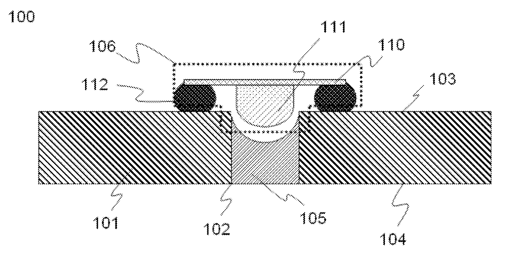
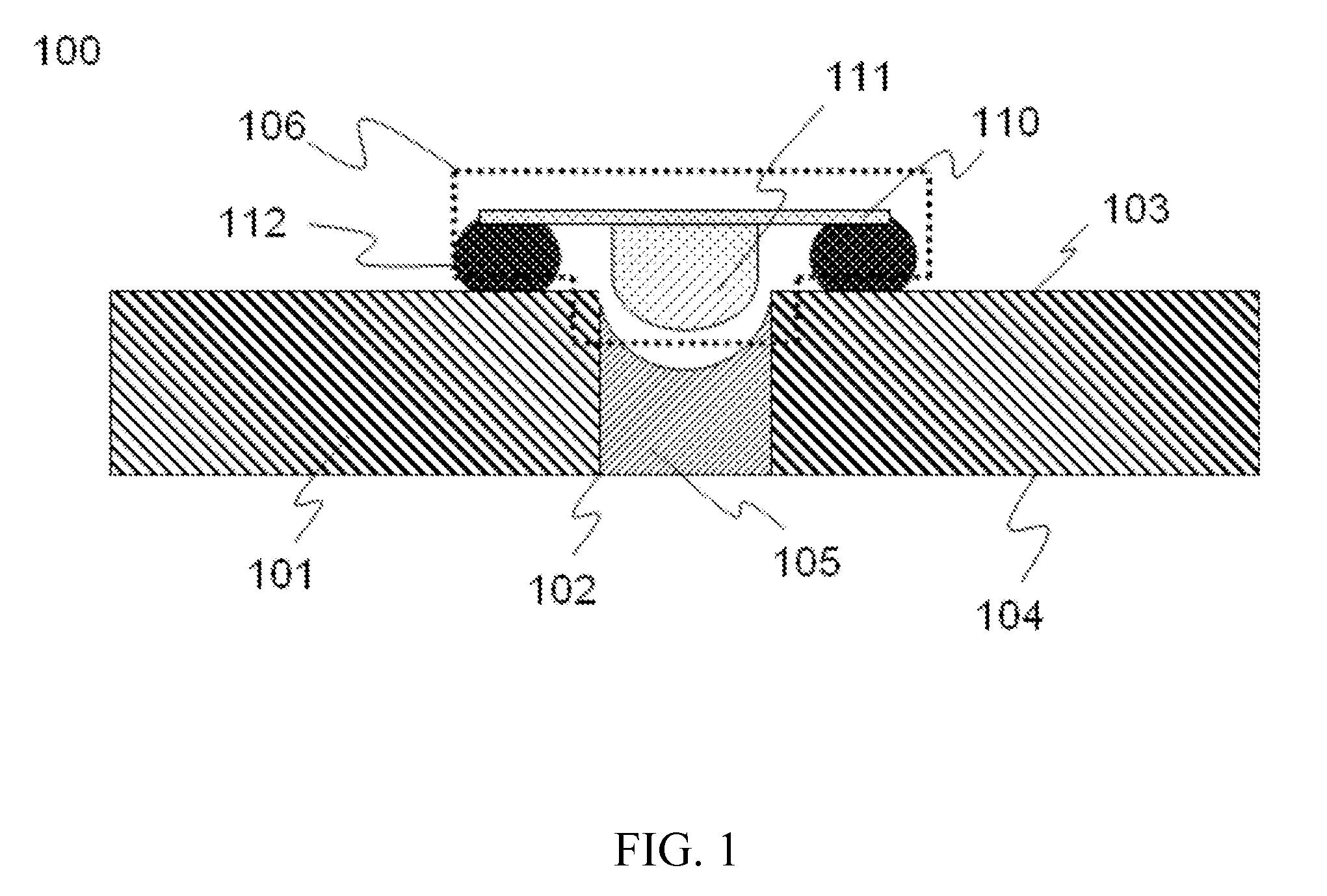
[0028]Please refer to FIG. 1. A micro electronic component structure 100 in the invention includes an insulating body 101, at least one through hole 102, at least one conductive material 105, and least one micro terminal 106. The insulating body 101 has a top surface 103 and a bottom surface 104. The conductive through hole 102 penetrates the top surface 103 and the bottom surface 104. The conductive material 105 is formed in the conductive through hole 102. The micro terminal 106 is disposed above the conductive material 105.

[0029]The conductive material 105 is formed in the conductive through hole 102 and forms a concave structure adjacent to the top surface 103; further, the top of the conductive material 105 is exposed to the top surface 103 of the insulating body 101. Similarly, the bottom of the conductive material 105 is exposed to the bottom surface 104 of the insulating body 101 to allow the micro terminal 106 to be electrically connected with other electronic components.

[0...

fourth embodiment

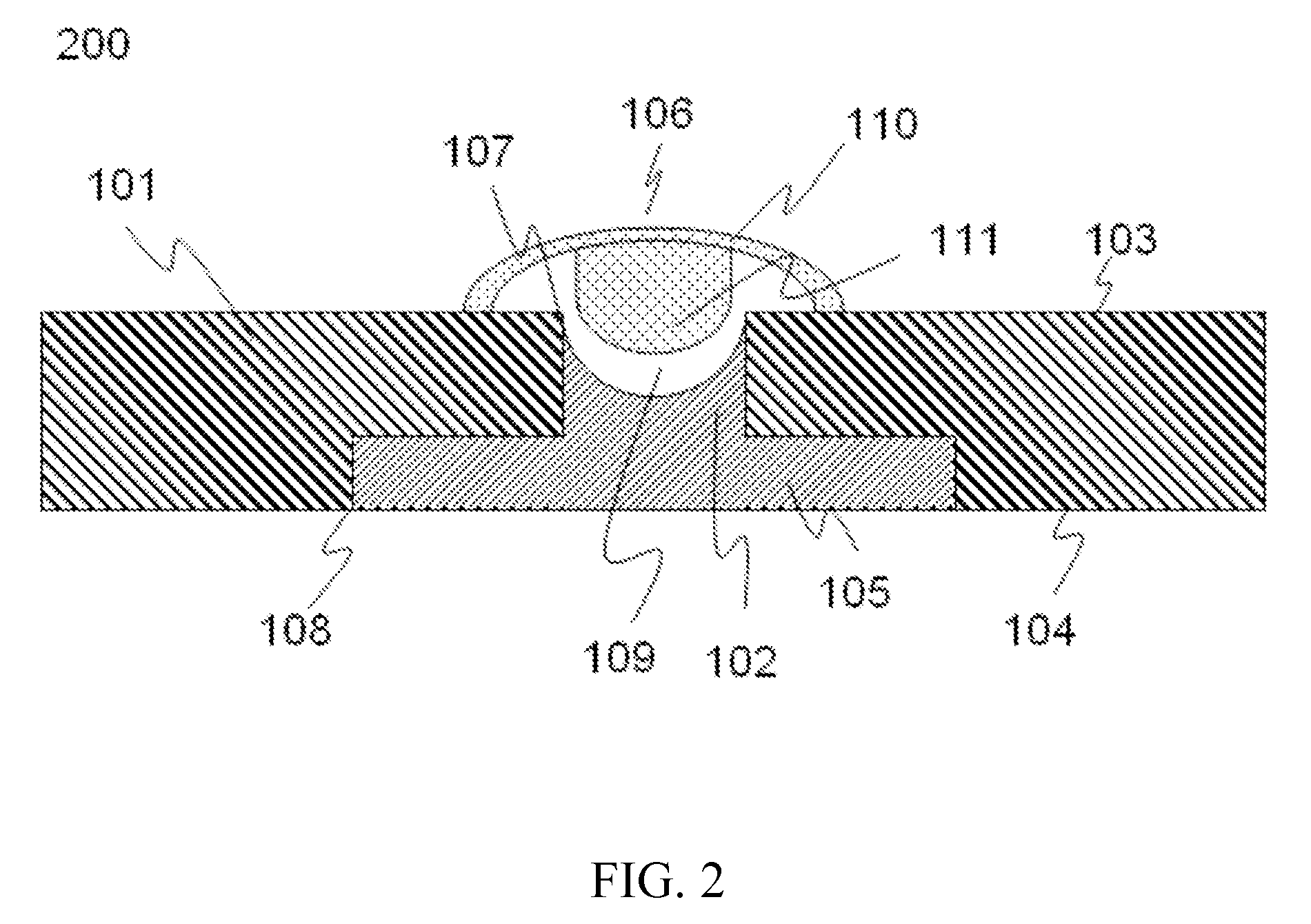
[0034]Please refer to FIG. 5 and FIG. 6. A micro electronic component structure 400 in the invention includes an insulating body 101, at least one conductive through hole 102, at least one conductive material 105, and at least one micro terminal 106.

[0035]The micro terminal 106 is disposed at the insulating body 101 in the method similar to the first embodiment, and it is not described for a concise purpose. In the embodiment, the micro electronic component structure 400 further includes a substrate 113 connected with the bottom surface 104. Further, the micro electronic component structure 400 further includes at least one connecting pad 114 disposed at or embedded in the substrate 113. The connecting pad 114 is disposed corresponding to the conductive material 105 for an electrical connection. Further, in the embodiment, the connecting pad 114 has an adhesive layer 115 formed thereon to enhance the connection strength between the micro electronic component structure 400 and the co...


PUM


Abstract

A micro electronic component structure includes an insulating body, at least one conductive through hole, at least one conductive material, and at least one micro terminal. The insulating body has a top surface and a bottom surface. The conductive through hole penetrates the top surface and the bottom surface. The conductive material is formed in the conductive through hole. The micro terminal is disposed above the conductive material.

Description

NOTICE OF COPYRIGHT[0001]A portion of the disclosure of this patent document contains material which is subject to copyright protection. The copyright owner has no objection to any reproduction by anyone of the patent disclosure, as it appears in the United States Patent and Trademark Office patent files or records, but otherwise reserves all copyright rights whatsoever.CROSS REFERENCE OF RELATED APPLICATION[0002]This Non-provisional application claims priority under 35 U.S.C. §119(a) on Patent Application No(s). 102201309 filed in Taiwan, Republic of China 201320046425.7, the entire contents of which are hereby incorporated by reference.BACKGROUND OF THE PRESENT INVENTION[0003]1. Field of Invention[0004]This invention relates to an electrical connection interface and, more particularly, to an electronic component structure of composite multi-factor deformation characteristics formed by a micro terminal made of an elastic material and a bonding material with an elastic effect.[0005]...

Claims


Application Information

Patent Timeline
Patent Type & Authority Patents(United States)
IPC IPC(8): H05K1/11H05K1/16H05K3/34
CPCH05K1/115H05K1/16H01H2207/04H01H2227/018H05K2201/10265H05K2201/09472H05K2201/09563H05K2201/1031H05K2201/10053H05K3/3436Y02P70/50
Inventor LIN, DIANN FANG
Owner KING YUAN ELECTRONICS
Why Eureka
Try Eureka