
SERS-active structure, fabrication method thereof, and SERS system comprising the same

a technology of active structure and sers, applied in the field of active structure, can solve the problems of low yield, narrow scope of generated hot spots, unconcentrated distribution, etc., and achieve the effect of low cost and low yield

Active Publication Date: 2015-09-08
NATIONAL TSING HUA UNIVERSITY
View PDF3 Cites 12 Cited by
  • Summary
  • Abstract
  • Description
  • Claims
  • Application Information

AI Technical Summary

Benefits of technology

This patent describes a surface structure that can enhance the detection of fluorescent molecules called Raman scatterers. This structure consists of a metal nanoparticle, a dielectric layer with a cavity, and a metal nanolayer with a gap. This structure can be used in a surface-enhanced Raman system (SERS) to improve the detection of analytes by generating a plasmonic field and detecting the scattered photons. The technical effect is a more efficient and accurate detection of analytes using a simple and effective surface structure.

Problems solved by technology

With the conventional SERS-active structure, the generated hot spots have drawbacks narrow scope and unconcentrated distribution.
Conventional fabrication methods for the SERS-active structures such as electron beam lithography and focused ion beam milling are at high cost but low yield because of the requirements of complicated steps and expensive apparatus.

Method used


Image

  • SERS-active structure, fabrication method thereof, and SERS system comprising the same
  • SERS-active structure, fabrication method thereof, and SERS system comprising the same
  • SERS-active structure, fabrication method thereof, and SERS system comprising the same

Examples


Embodiment Construction

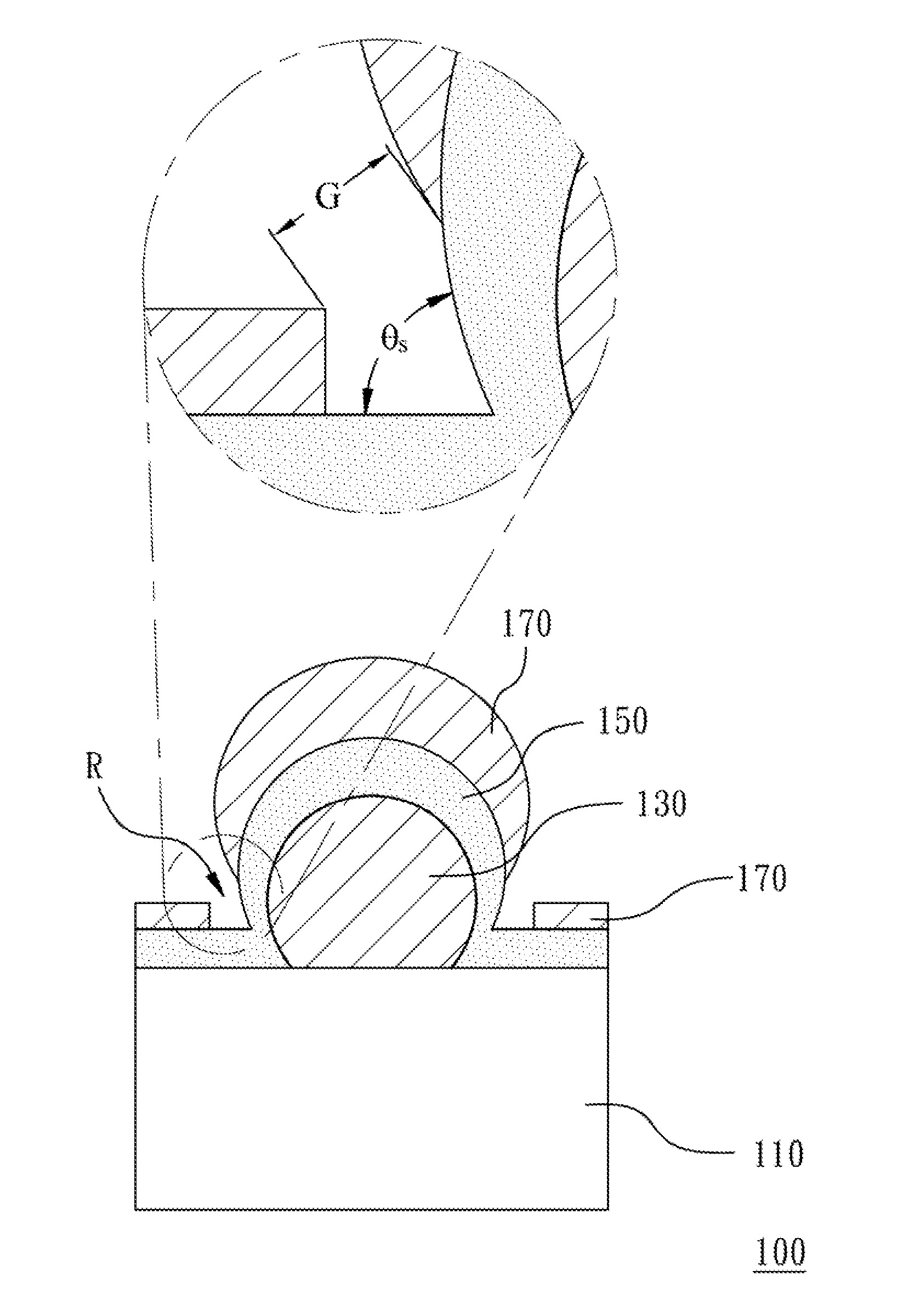
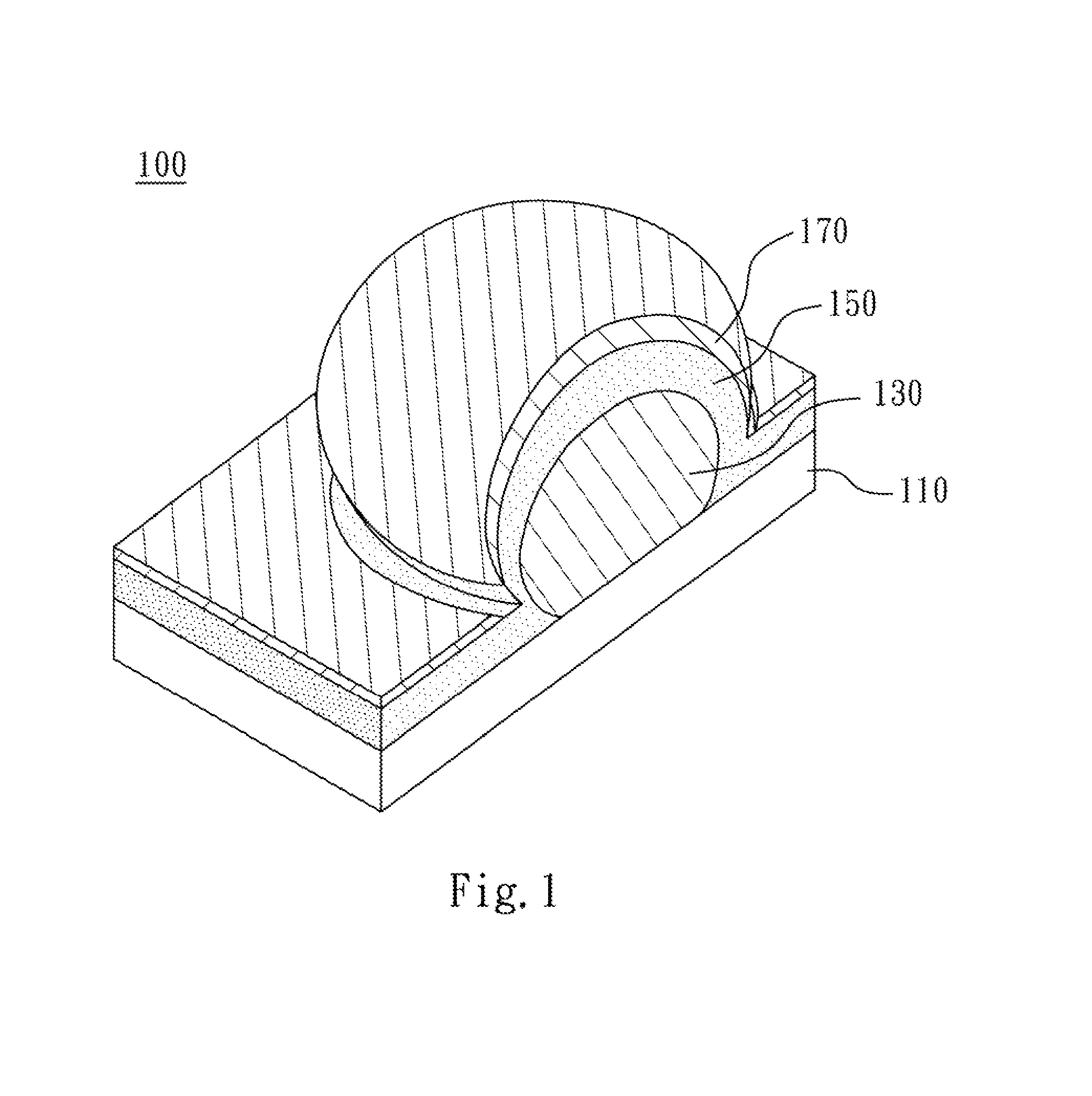
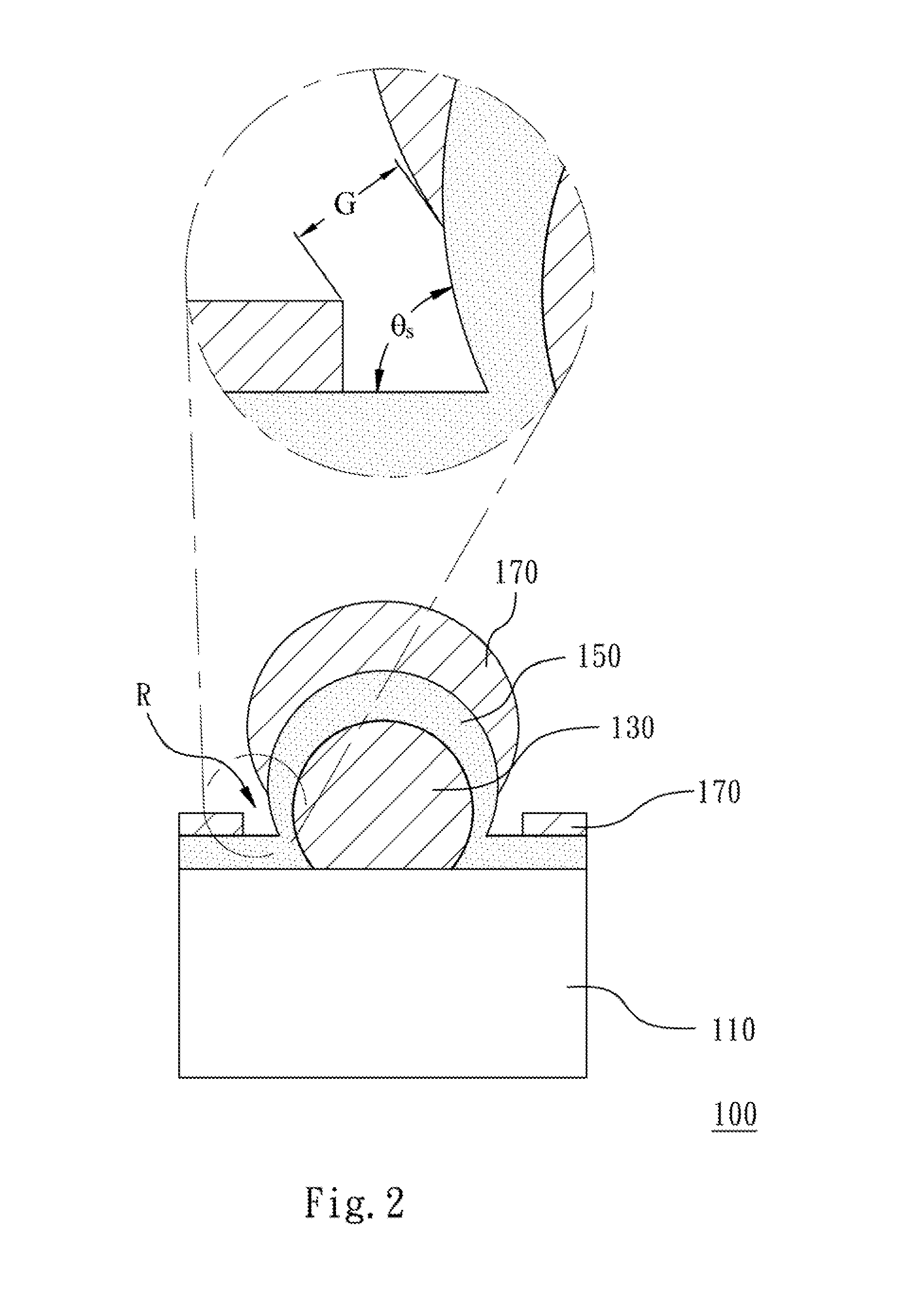
[0021]FIG. 1 is a partial schematic view showing a SERS-active structure according to one embodiment of the present disclosure. FIG. 2 is a sectional view of FIG. 1. Please refer to FIG. 1 and FIG. 2, a SERS-active structure 100 includes a substrate 110, at least one metal nanoparticle 130, a dielectric layer 150, and a metal nanolayer 170 (i.e. a metal layer in nanoscale). The at least one metal nanoparticle 130 is disposed on the substrate 110. The dielectric layer 150 covers the substrate 100 and the at least one metal nanoparticle 130, so that the dielectric layer 150 forms a recessed portion R which has a dihedral angle θs. That is to say, the dielectric layer 150 includes a recessed portion R with a dihedral angle θs formed by a surface of the dielectric layer 150 where the at least one metal nanoparticle 130 contacts the substrate 110. The metal nanolayer 170 covers the dielectric layer 150 and has a gap G located at and exposing the recessed portion R. The dihedral angle θs ...


PUM

PropertyMeasurementUnit
widthaaaaaaaaaa
widthaaaaaaaaaa
thicknessaaaaaaaaaa

Abstract

A SERS-active structure includes a substrate, at least one metal nanoparticle, a dielectric layer and a metal nanolayer. The metal nanoparticles are disposed on the substrate. The substrate and the metal nanoparticles are covered by the dielectric layer, so that the dielectric layer forms a recessed portion with a dihedral angle formed by a surface of the dielectric layer at which the at least one metal nanoparticle contacts the substrate. The dielectric layer is covered by the metal nanolayer and the metal nanolayer has a gap located at and exposing the recessed portion.

Description

RELATED APPLICATIONS[0001]This application claims priority to Taiwan Patent Application Serial Number 101128798, filed Aug. 9, 2012, which is herein incorporated by reference.BACKGROUND[0002]1. Field of Invention[0003]The present disclosure relates to an active structure. More particularly, the present disclosure relates to a surface-enhanced Raman scattering (SERS)-active structure, a method for fabricating the SERS-active structure, and a SERS system comprising the SERS-active structure.[0004]2. Description of Related Art[0005]Surface-enhanced Raman scattering (SERS) is a technique concerning surface effects. The SERS technique is able to significantly enhance the Raman signal from analyte molecules, by such as adsorbed or adjacently jointed over a metal surface. In this regard, a structure is capable of enhancing the Raman signal of the analyte molecules over the metal surface is so called a SERS-active structure.[0006]The SERS technique mainly applies the property of nanoscale m...

Claims


Application Information

Patent Timeline
Patent Type & Authority Patents(United States)
IPC IPC(8): G01J3/44B32B3/10B05D7/22H03F17/00G01J1/58G01N21/65
CPCG01J3/44G01N21/658
Inventor TSENG, FAN-GANGKUO, TENG-FENGLEE, TSUNG-YEN
Owner NATIONAL TSING HUA UNIVERSITY
Learn More