[0009]In the in-cell liquid crystal display device having a built-in touch panel, it is possible to reduce the number of components by forming a liquid crystal display panel driver IC, which drives the liquid crystal display panel, and a touch panel driver IC, which detects a touch position, as a common driver.
[0011]The liquid crystal display device detects the touch position on the touch panel even in a standby state. Hence, there is a problem in that, in the standby state, the liquid crystal display device is in a display off state in which “black” is displayed on the liquid crystal display panel but nevertheless it is difficult to reduce power consumption in the liquid crystal display device.
[0012]The invention has been made to solve the problem in the related art, and it is an object of the invention to provide a technique, which is capable of reducing power consumption in the liquid crystal display device at the time when the display is off, which displays “black” on the liquid crystal display panel in the standby state, for the in-cell liquid crystal display device having the touch panel function.
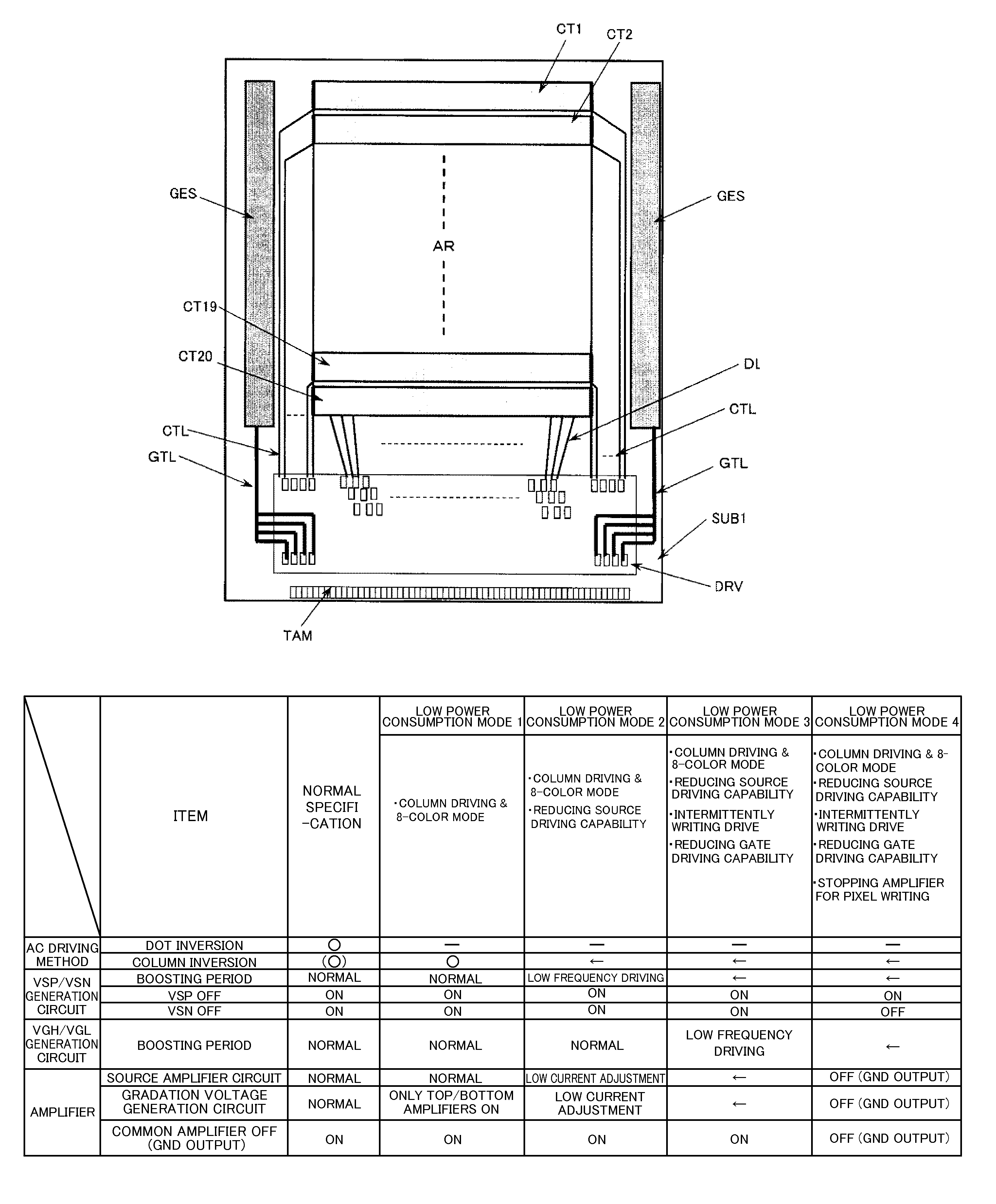
[0016](2) According to a second aspect of the invention, there is provided a liquid crystal display device including a liquid crystal display panel that has a first substrate, a second substrate, and a liquid crystal sandwiched between the first substrate and the second substrate, in which there is provided a display section formed of a plurality of pixels arranged in matrix, wherein the second substrate has detection electrodes of a touch panel, wherein each pixel has a pixel electrode and a counter electrode, wherein the display section is divided into a plurality of blocks each of which is formed of the pixels disposed on a plurality of display lines adjacent to one another, wherein the counter electrode is an electrode common to the pixels in each block, wherein the counter electrode of each block also functions as a scanning electrode of the touch panel, wherein the liquid crystal display device has a driving circuit which supplies a counter voltage and a touch panel scanning voltage to the counter electrodes of the respective blocks, wherein the driving circuit has a common amplifier circuit which supplies the counter voltage to the counter electrodes, wherein the common amplifier circuit has a current adjustment circuit capable of adjusting current flowing in the common amplifier circuit itself, and wherein the driving circuit causes the current adjustment circuit to stop an operation of the common amplifier circuit and supply a GND voltage to the counter electrodes in a low power consumption mode for achieving lower power consumption than a normal operation.
[0017](3) According to a third aspect of the invention, there is provided a liquid crystal display device including a liquid crystal display panel that has a first substrate, a second substrate, and a liquid crystal sandwiched between the first substrate and the second substrate, in which there is provided a display section formed of a plurality of pixels arranged in matrix, wherein the second substrate has detection electrodes of a touch panel, wherein each pixel has a pixel electrode and a counter electrode, wherein the display section is divided into a plurality of blocks each of which is formed of the pixels disposed on a plurality of display lines adjacent to one another, wherein the counter electrode is an electrode common to the pixels in each block, wherein the counter electrode of each block also functions as a scanning electrode of the touch panel, wherein the liquid crystal display device has a driving circuit which supplies a counter voltage and a touch panel scanning voltage to the counter electrodes of the respective blocks, wherein the driving circuit has a gradation voltage generation circuit which generates a plurality of gradation voltages, wherein the gradation voltage generation circuit has a plurality of amplifier circuits which output the plurality of gradation voltages, wherein each amplifier circuit has a current adjustment circuit capable of adjusting current flowing in the amplifier circuit itself, and wherein the driving circuit causes the current adjustment circuit of a middle amplifier circuit other than a top amplifier circuit, which outputs a highest gradation voltage, and a bottom amplifier circuit, which outputs a lowest gradation voltage, among the plurality of amplifier circuits, to stop an operation of the corresponding middle amplifier circuit, in a first low power consumption mode for achieving lower power consumption than a normal operation, causes the current adjustment circuit of the middle amplifier circuit to stop the operation of the corresponding middle amplifier circuit and causes the current adjustment circuits of the top amplifier circuit and the bottom amplifier circuit to reduce current, which flows in the top amplifier circuit and the bottom amplifier circuit, such that the current is lower than current, which flows in the amplifier circuit at the time of the normal operation, in a second low power consumption mode for achieving lower power consumption than the first low power consumption mode, and causes the current adjustment circuits of the respective amplifier circuits, which output the plurality of gradation voltages, to stop operations of the respective amplifier circuits and supply a GND voltage as the lowest gradation voltage, in a third low power consumption mode for achieving lower power consumption than the second low power consumption mode.
[0021]According to the liquid crystal display device having the touch panel function of the invention, it is possible to reduce power consumption in the liquid crystal display device at the time when the display is off which displays “black” on the liquid crystal display panel in the standby state.
