
Wire, method of manufacture, and related apparatus

a manufacturing method and wire technology, applied in the direction of instruments, static indicating devices, conductive pattern formation, etc., can solve problems such as disconnection defects, and achieve the effects of preventing disconnection of wires, thin thickness, and reducing the step difference between various elements of the first substra

Active Publication Date: 2015-06-16
SAMSUNG DISPLAY CO LTD
View PDF7 Cites 0 Cited by
  • Summary
  • Abstract
  • Description
  • Claims
  • Application Information

AI Technical Summary

Benefits of technology

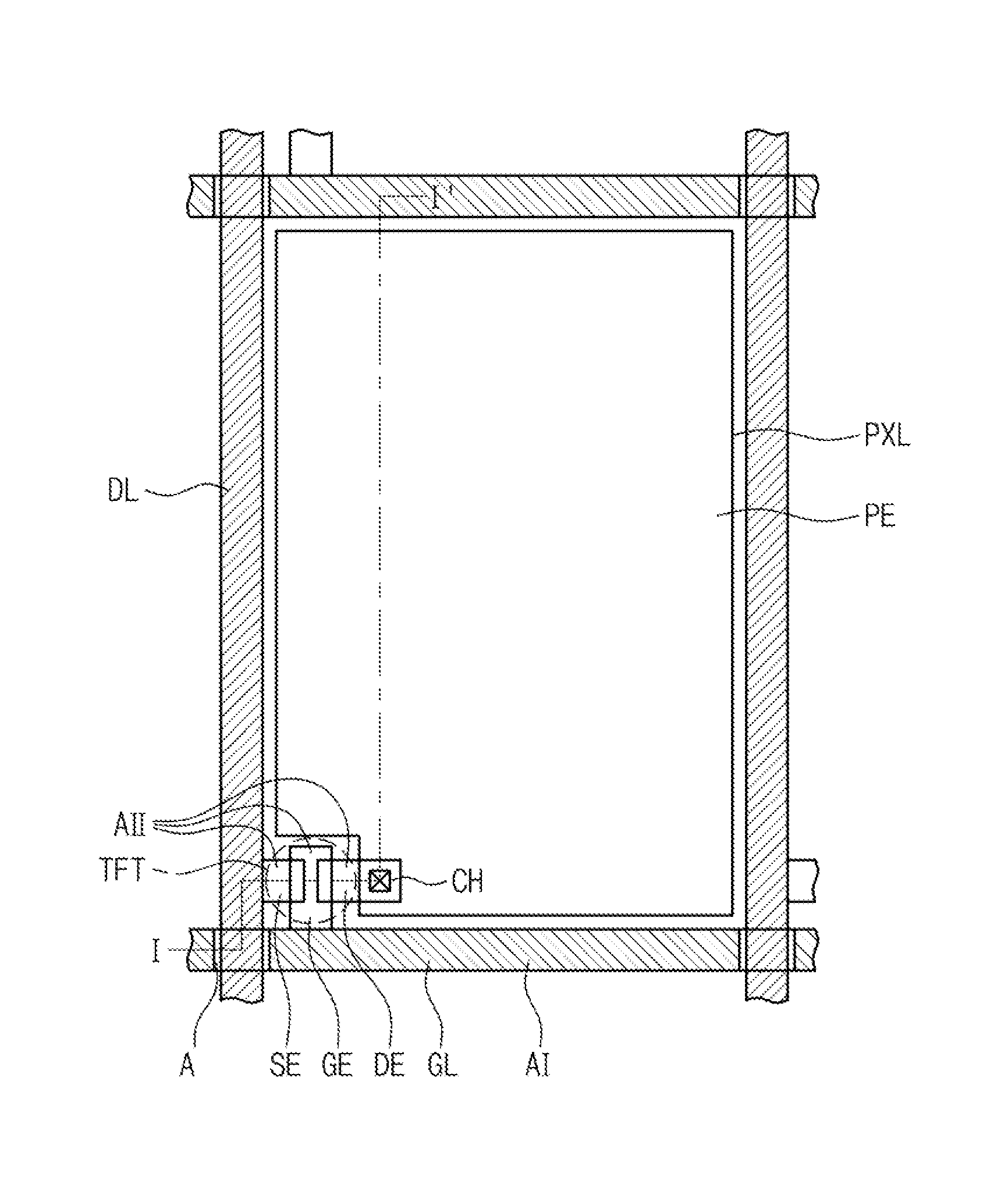
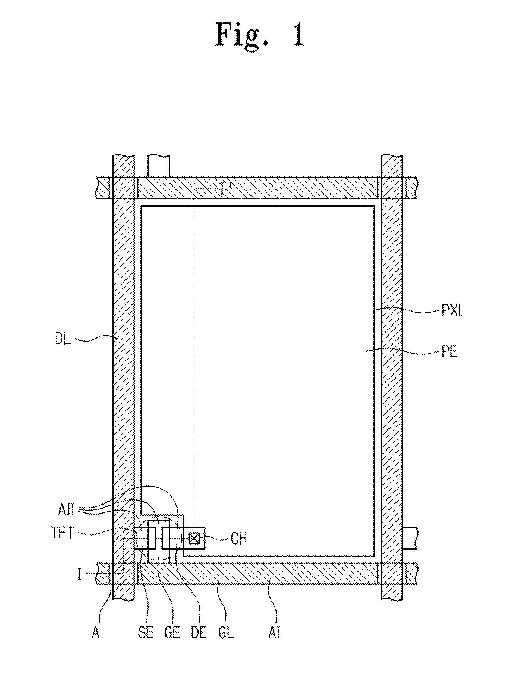
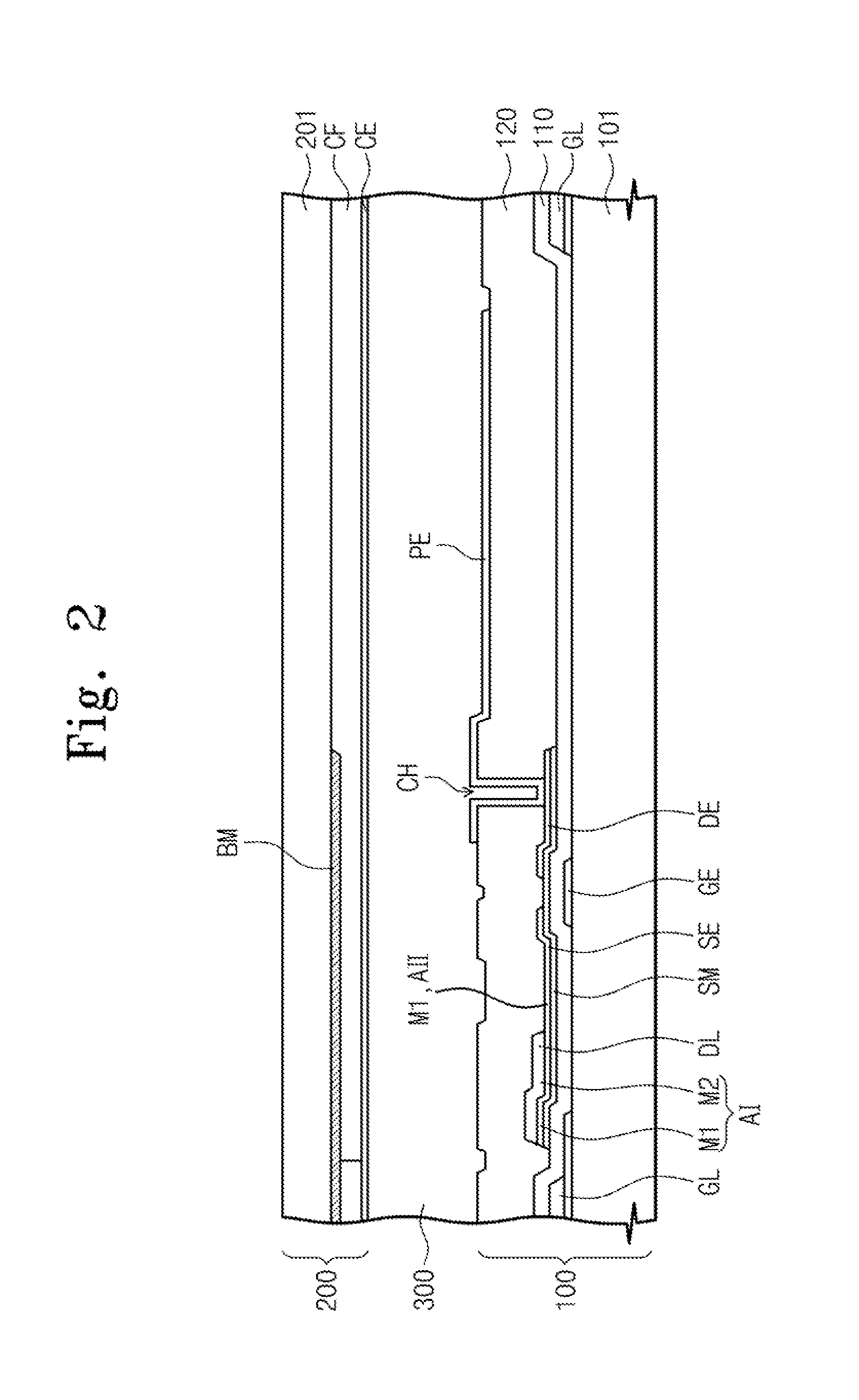
[0008]In the display apparatus according to an exemplary embodiment, the thickness of the wires in which plural layers are stacked may be controlled, thereby preventing the wire from being disconnected. In an exemplary embodiment, each of the wires formed in the area in which the wires are stacked has a relatively thin thickness. Accordingly, although multiple wires are stacked in the area, the step difference between various elements for the first substrate may be reduced, thereby preventing disconnection of the wires.
[0009]In one exemplary embodiment, since the wire has a different thickness according to different areas, the disconnection of the wire may be prevented even though the wire is overlapped with others.
[0010]In one exemplary embodiment, a display apparatus employs the wire to prevent the wire from being disconnected. In addition, the wire may be patterned by a single photolithography process, so the manufacturing time and cost for the wire may be reduced. Further, in the display apparatus, each of a first and a second wire part may be formed to have different thicknesses using four masks, to thereby reduce manufacturing time and cost for the display apparatus.

Problems solved by technology

In the case that each wire has uniform thickness throughout its length, a disconnection defect may occur in the overlap area in which the gate line GL overlaps with the data line DL or where the thin film transistor is formed due to a step difference between the area in which the wires are stacked and the area in which the wires are not formed.

Method used


Image

  • Wire, method of manufacture, and related apparatus
  • Wire, method of manufacture, and related apparatus
  • Wire, method of manufacture, and related apparatus

Examples


Embodiment Construction

[0021]It will be understood that when an element or layer is referred to as being “on”, “connected to” or “coupled to” another element or layer, it can be directly on, connected or coupled to the other element or layer or intervening elements or layers may be present. In contrast, when an element is referred to as being “directly on,”“directly connected to” or “directly coupled to” another element or layer, there are no intervening elements or layers present. Like numbers refer to like elements throughout. As used herein, the term “and / or” includes any and all combinations of one or more of the associated listed items.

[0022]It will be understood that, although the terms first, second, etc. may be used herein to describe various elements, components, regions, layers and / or sections, these elements, components, regions, layers and / or sections should not be limited by these terms. These terms are only used to distinguish one element, component, region, layer or section from another reg...


PUM

PropertyMeasurementUnit
thicknessaaaaaaaaaa
thicknessaaaaaaaaaa
thicknessaaaaaaaaaa

Abstract

A wire is provided on an insulating substrate to have a first thickness in a first area and a second thickness smaller than the first thickness in a second area except for the first area. A display apparatus includes the wire. The wire is formed by forming a first conductive layer and a second conductive layer on the insulating substrate and etching the first and second conductive layers using photoresist layer patterns having different thicknesses.

Description

CROSS-REFERENCE TO RELATED APPLICATION[0001]This application relies for priority upon Korean Patent Application No. 10-2010-0097923 filed on Oct. 7, 2010, the contents of which are herein incorporated by reference in its entirety.BACKGROUND[0002]1. Field of Disclosure[0003]The subject matter disclosed herein relates to a wire, a method of manufacturing the wire, a display apparatus having the wire, and a method of manufacturing the display apparatus.[0004]2. Description of the Related Art[0005]A liquid crystal display is one of the most widely used flat panel displays. The liquid crystal display includes two substrates and a liquid crystal layer interposed between the two substrates. The liquid crystal display applies an electric field to the liquid crystal layer to rearrange liquid crystal molecules of the liquid crystal layer, thereby controlling light amount of the light passing through the liquid crystal layer.[0006]Electrodes and wires connected to the electrodes are arranged o...

Claims


Application Information

Patent Timeline
Patent Type & Authority Patents(United States)
IPC IPC(8): G02F1/136G02F1/1343G02F1/1362
CPCG02F1/136286Y10T29/49155G02F2001/136236G02F2001/136295G02F2201/123G02F1/136236G02F1/136295G02F1/136227H01L27/1288
Inventor CHANG, CHONG SUPKHANG, YOONHOJEONG, CHANGOHYU, SEHWANPARK, SANGHOKANG, SU-HYOUNGKIM, HYUNGJUNNING, HONGLONGHWANG, JINHOCHA, MYOUNGGEUNSHIN, YOUNGKI
Owner SAMSUNG DISPLAY CO LTD
Learn More