Electro-static-discharge (ESD) protection structure with stacked implant junction transistor and parallel resistor and diode paths to lower trigger voltage and raise holding volatge

a protection structure and electrostatic discharge technology, applied in the direction of transistors, electrical apparatus, semiconductor devices, etc., can solve the problems of esd failure in the factory, prone to damage and failure of integrated circuits (ic's), and lowering yields

Active Publication Date: 2015-06-09
HONG KONG APPLIED SCI & TECH RES INST
View PDF11 Cites 5 Cited by
  • Summary
  • Abstract
  • Description
  • Claims
  • Application Information

AI Technical Summary

Problems solved by technology

Integrated circuits (IC's) are prone to damage and failure from an electro-static-discharge (ESD).
ESD failures may occur in the factory and contribute to lower yields.
These smaller transistors are much more susceptible to over-voltage failure but can operate with a lower power-supply voltage, thus consuming less power and producing less heat.
Static charges from a person or machinery can produce such damaging currents that are only partially blocked by the input-protection circuits in the periphery.
Then thermal breakdown occurs as portions of the transistor may melt or otherwise be permanently damaged.
Thus high-voltage transistors are not effective in protecting low-voltage transistors in low-voltage core circuitry 20.
This design window may be relatively small and difficult to achieve.
Some prior-art ESD protection structures have large-area capacitors, resistors, or transistors which are undesirable.
Unfortunately, breakdown voltages may still be less than trigger voltages, allowing damage to occur despite the ESD implant.
Leakage may be a problem for some structures, especially diode or diode-triggered structures.
Leakage from p-n junctions is sometimes a problem with some ESD protection devices.

Method used


Image

  • Electro-static-discharge (ESD) protection structure with stacked implant junction transistor and parallel resistor and diode paths to lower trigger voltage and raise holding volatge
  • Electro-static-discharge (ESD) protection structure with stacked implant junction transistor and parallel resistor and diode paths to lower trigger voltage and raise holding volatge
  • Electro-static-discharge (ESD) protection structure with stacked implant junction transistor and parallel resistor and diode paths to lower trigger voltage and raise holding volatge

Examples


Embodiment Construction

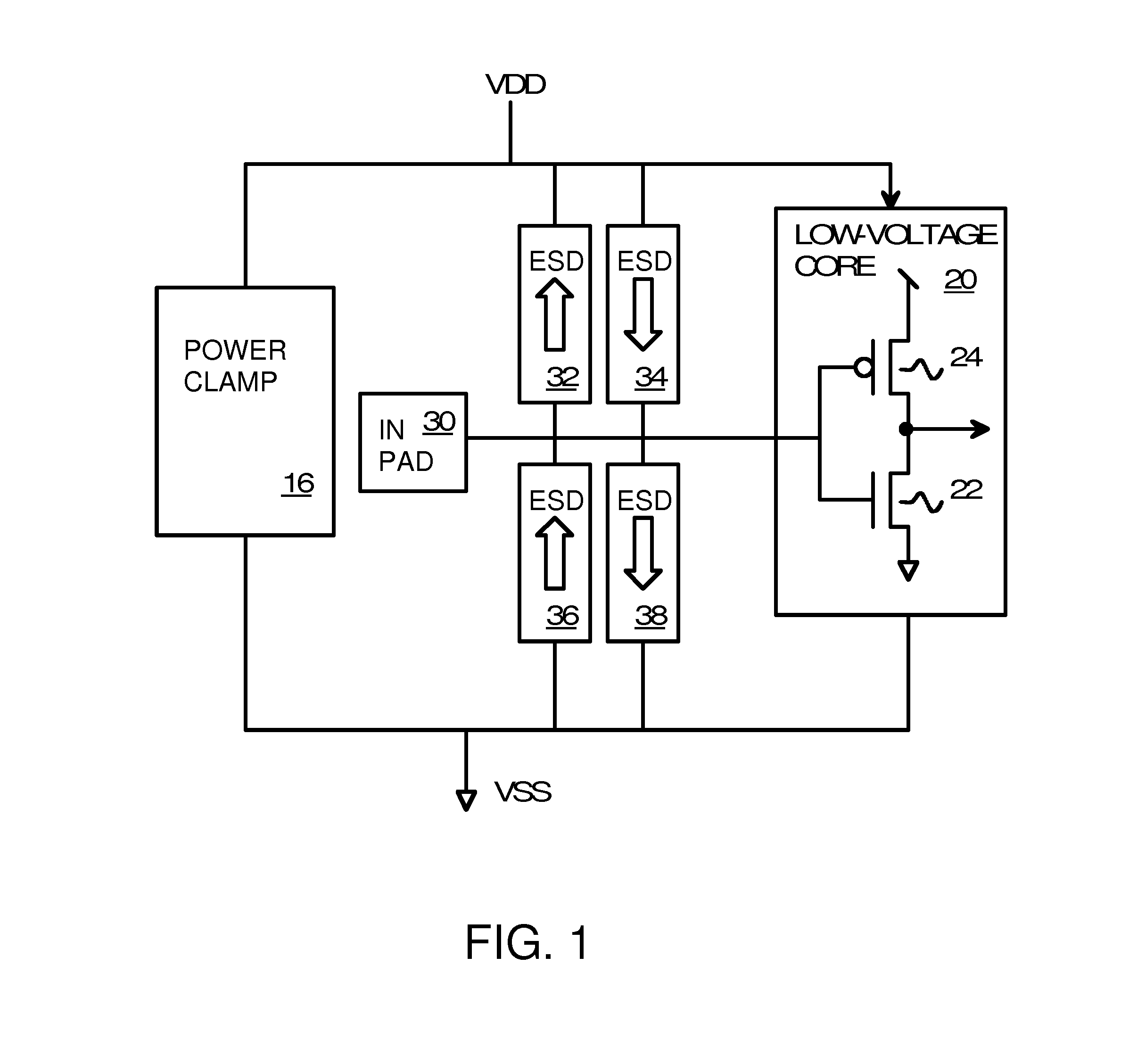
[0026]The present invention relates to an improvement in ESD protection circuits. The following description is presented to enable one of ordinary skill in the art to make and use the invention as provided in the context of a particular application and its requirements. Various modifications to the preferred embodiment will be apparent to those with skill in the art, and the general principles defined herein may be applied to other embodiments. Therefore, the present invention is not intended to be limited to the particular embodiments shown and described, but is to be accorded the widest scope consistent with the principles and novel features herein disclosed.

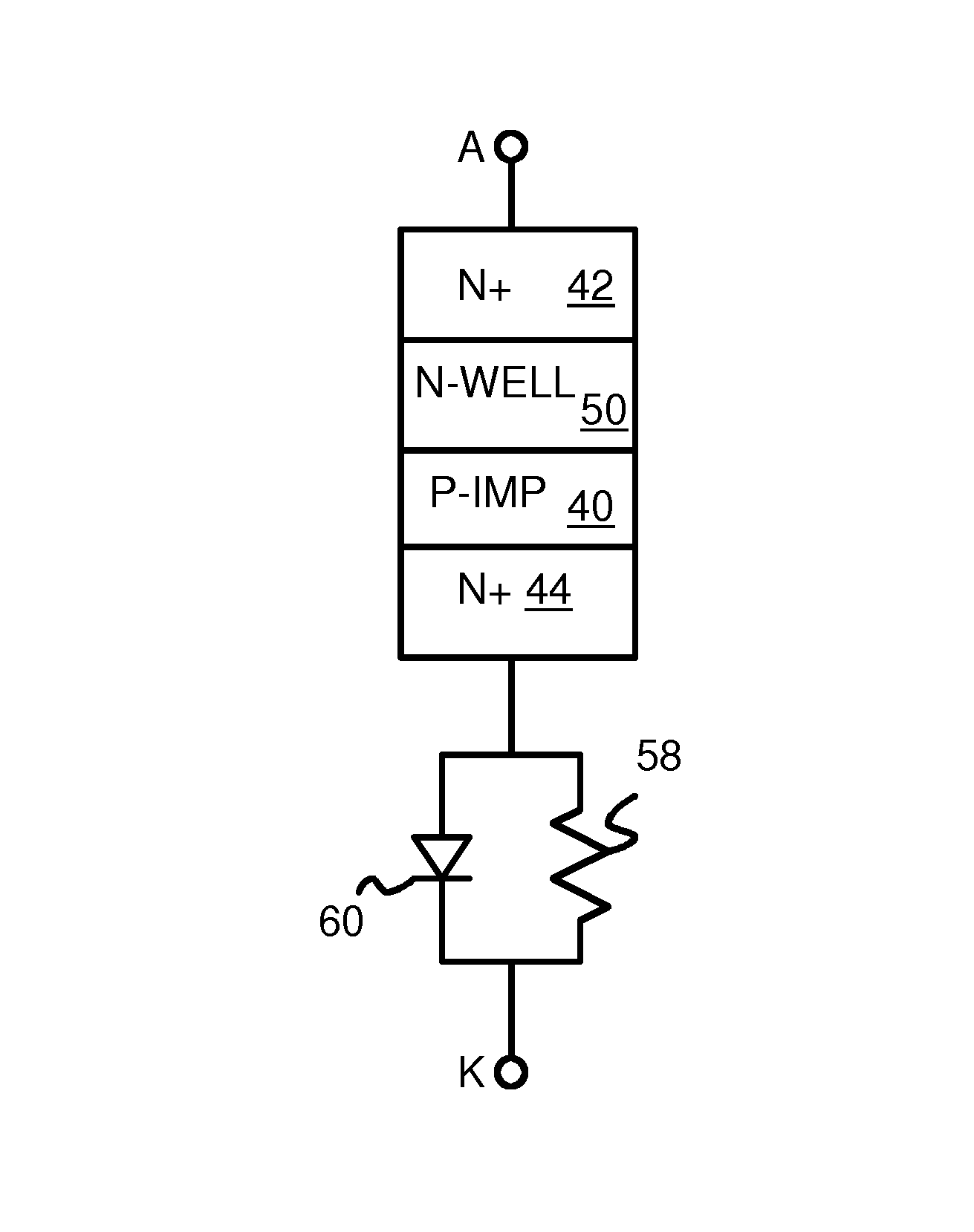
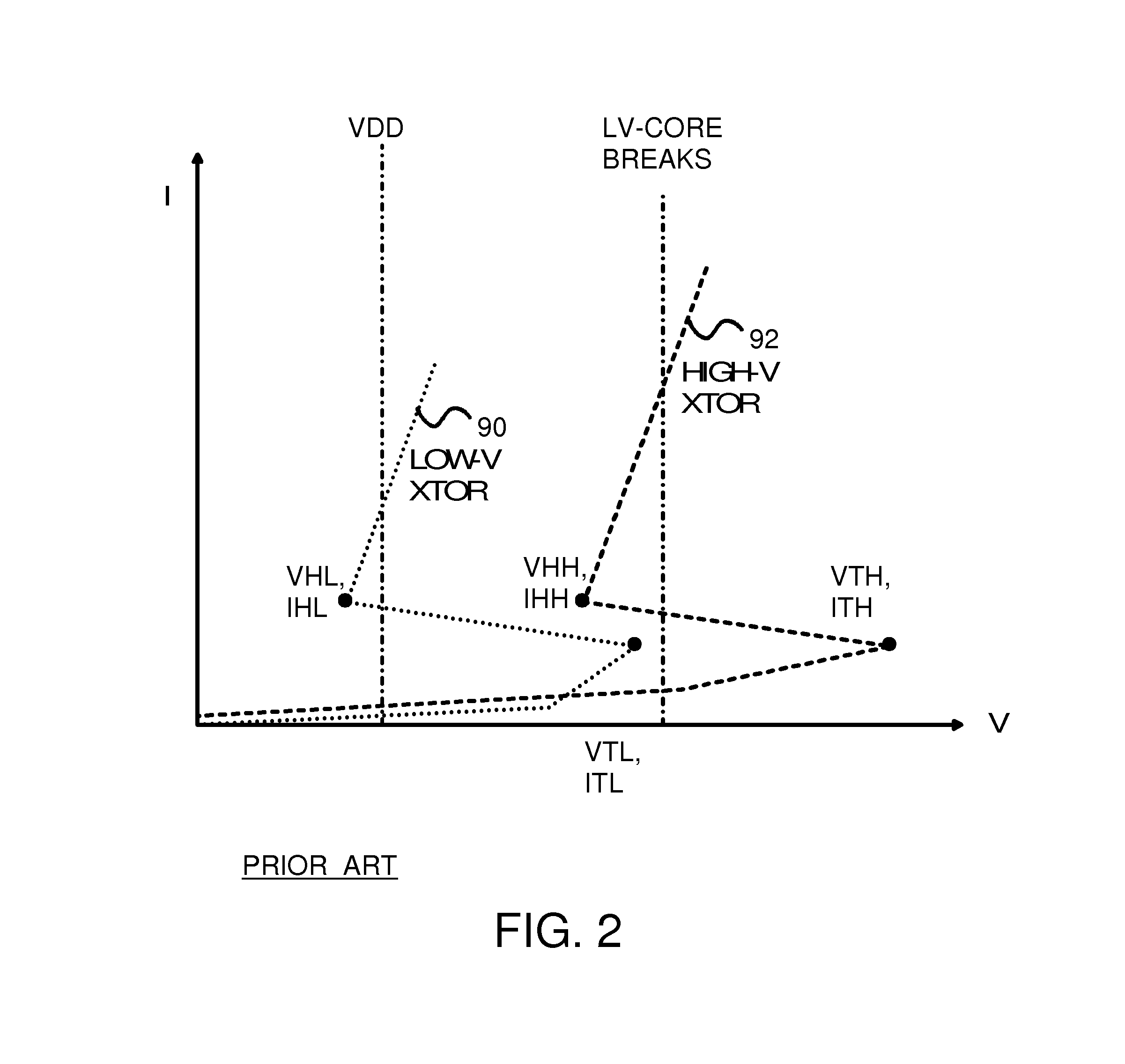
[0027]The inventors realize that an ESD implant may help to lower the trigger voltage, but the holding voltage may still be too low. The inventors realize that the holding voltage may be increased by adding a resistor path in parallel with a diode path. The resistor path sets the trigger voltage, while the diode path shunts a ...


PUM


Abstract

An electro-static-discharge (ESD) protection circuit has a vertical NPN transistor with a floating p-type base created by a deep p-type implant under an N+ source region. The deep p-type implant may be an ESD implant in a standard CMOS process. The p-type implant provides a low initial snap-back trigger voltage, but the holding voltage may be too low, creating latch-up problems. The holding voltage is raised by about one volt by connecting the emitter of the vertical NPN transistor to parallel resistor and diode paths. When the vertical NPN transistor is triggered, its current initially flows through the resistor, creating an increasing voltage drop through the resistor as current rises. Once the voltage across the resistor reaches 0.5 volt, the diode in parallel with the resistor becomes forward biased and shunts a higher current than the resistor, raising the holding voltage. A clamp transistor may replace the diode.

Description

FIELD OF THE INVENTION[0001]This invention relates to electro-static-discharge (ESD) protection circuits, and more particularly to snap-back devices using a deep p-type implant under a drain region.BACKGROUND OF THE INVENTION[0002]Integrated circuits (IC's) are prone to damage and failure from an electro-static-discharge (ESD). ESD failures may occur in the factory and contribute to lower yields. Various ESD-protection structures have been placed near input, output, or bi-directional I / O pins of ICs. Many of these protection structures use passive components such as series resistors, diodes, and thick-oxide transistors. Other ESD structures use an active transistor to safely shunt ESD current.[0003]As manufacturing ability improves and device sizes shrink, lower voltages are applied to transistors during normal operation. These smaller transistors are much more susceptible to over-voltage failure but can operate with a lower power-supply voltage, thus consuming less power and produc...

Claims


Application Information

Patent Timeline
Patent Type & Authority Patents(United States)
IPC IPC(8): H02H9/00H02H9/04H01L27/02
CPCH02H9/046H01L27/0248H01L27/0259
Inventor HUO, XIAOYAN, BEIPINGCAI, XIAOWU
Owner HONG KONG APPLIED SCI & TECH RES INST
Why Eureka
Try Eureka