
Recessed transistor and method of manufacturing the same

a technology of recessed transistors and transistors, which is applied in the direction of basic electric elements, electrical apparatus, semiconductor devices, etc., can solve the problems of undesirable wing characteristics, achieve the effects of reducing the occurrence, preventing (or reducing) the occurrence, and suppressing undesirable electrical characteristics of recessed transistors caused by the profile of the lower recess

Active Publication Date: 2015-04-21
SAMSUNG ELECTRONICS CO LTD
View PDF15 Cites 0 Cited by
  • Summary
  • Abstract
  • Description
  • Claims
  • Application Information

AI Technical Summary

Benefits of technology

The design enhances electrical characteristics of the recessed transistor by stabilizing channel formation and reducing the influence of the lower recess profile on swing characteristics, leading to improved performance.

Problems solved by technology

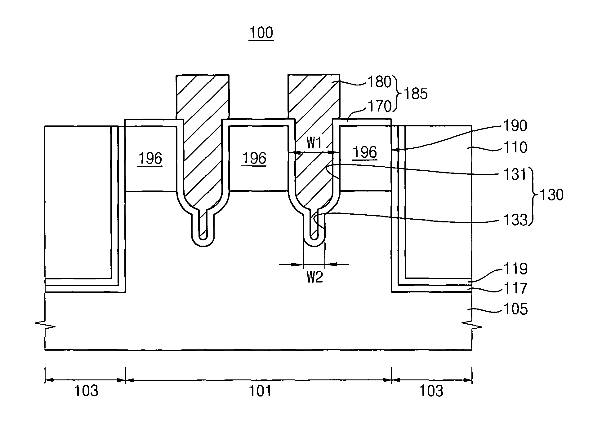
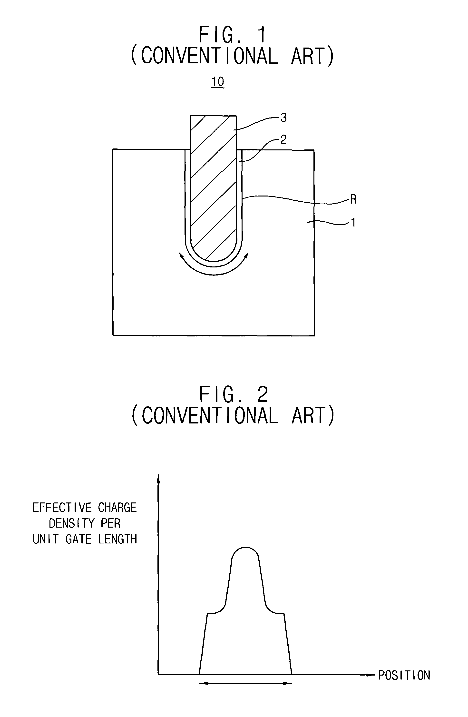
The effective charge density per the unit gate length may change substantially according to a profile of the gate insulation layer (indicated by arrows in FIGS. 1 and 2) on the bottom surface of the recess such that swing characteristics are undesirable.

Method used


Image

  • Recessed transistor and method of manufacturing the same
  • Recessed transistor and method of manufacturing the same
  • Recessed transistor and method of manufacturing the same

Examples


Embodiment Construction

[0037]Various example embodiments will now be described more fully with reference to the accompanying drawings in which some example embodiments are shown. In the drawings, the thickness of layers and regions may be exaggerated for clarity.

[0038]Detailed illustrative embodiments are disclosed herein. However, specwhenic structural and functional details disclosed herein are merely representative for purposes of describing example embodiments. This invention may, however, may be embodied in many alternate forms and should not be construed as limited to only example embodiments set forth herein.

[0039]Accordingly, while example embodiments are capable of various modwhenications and alternative forms, embodiments thereof are shown by way of example in the drawings and will herein be described in detail. It should be understood, however, that there is no intent to limit example embodiments to the particular forms disclosed, but on the contrary, example embodiments are to cover all modwhe...


PUM


Abstract

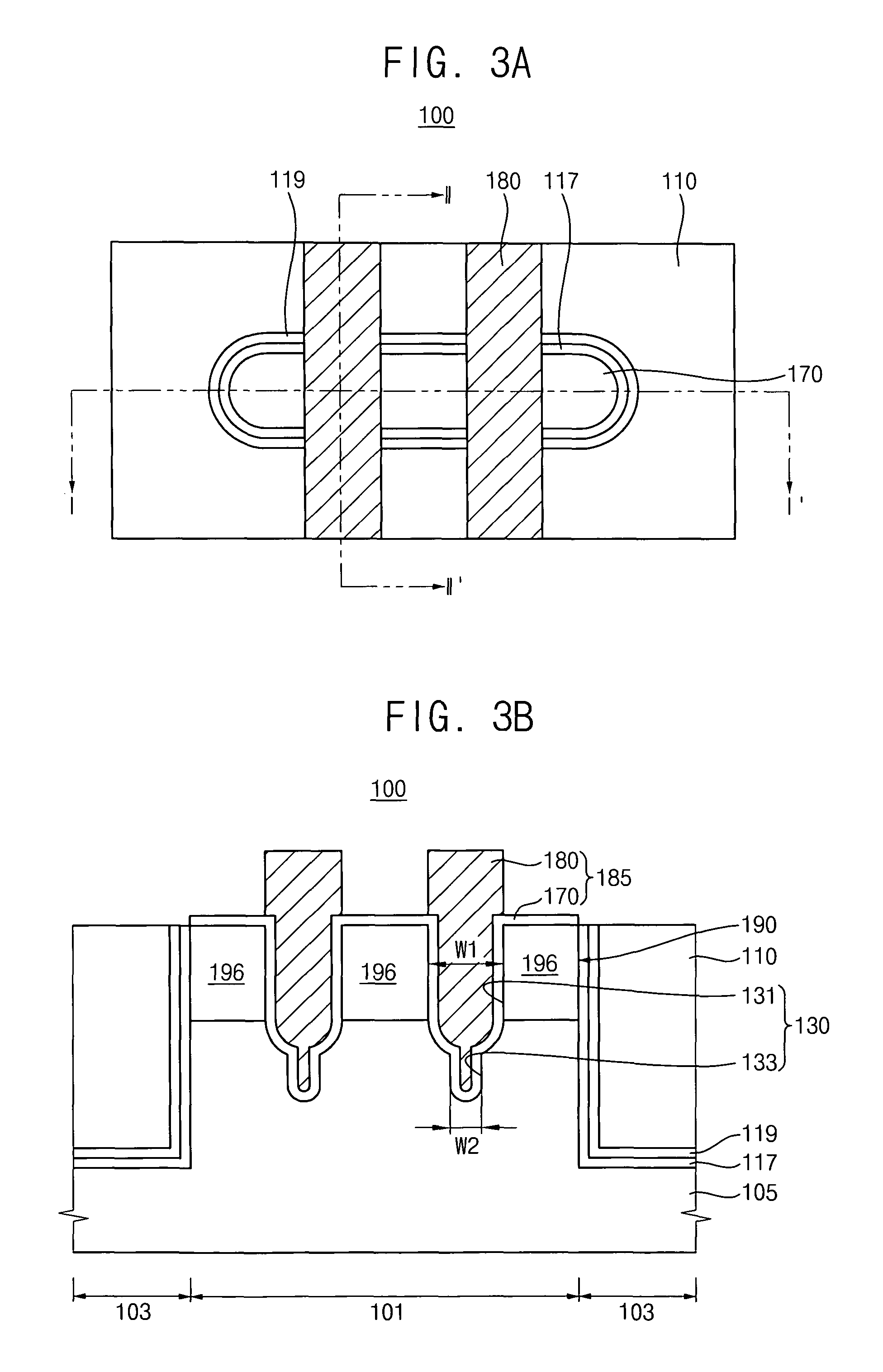
A recessed transistor and a method of manufacturing the same are provided. The recessed transistor may include a substrate, an active pin, a gate pattern and source and drain regions. The substrate may include an isolation layer that establishes an active region and a field region of the substrate. The substrate may include a recessed structure having an upper recess formed in the active region and a lower recess in communication with the upper recess. An active pin may be formed in a region between side surfaces of the isolation layer and the lower recess and an interface between the active region and the field region. The gate pattern may include a gate insulation layer formed on an inner surface of the recessed structure and a gate electrode formed on the gate insulation layer in the recessed structure. The source / drain regions may be formed adjacent to the active region and the gate electrode.

Description

PRIORITY STATEMENT[0001]This application claims the benefit of priority under 35 U.S.C. §119 to Korean Patent Application No. 2007-11527, filed on Feb. 5, 2007 in the Korean Intellectual Property Office (KIPO), the contents of which are herein incorporated by reference in their entirety.BACKGROUND[0002]1. Field[0003]Example embodiments relate to a recessed transistor and a method of manufacturing the same. Other example embodiments relate to a recessed transistor including a gate structure that is formed in a recessed structure of an active region and a method of manufacturing the recessed transistor.[0004]2. Description of the Related Art[0005]As semiconductor devices become more highly integrated, it is desirable to decrease widths of each pattern and the intervals between the patterns of the semiconductor device. In order to decrease the width (and intervals) of each pattern, it is desirable to obtain a more precisely and accurately formed minute pattern. In the semiconductor dev...

Claims


Application Information

Patent Timeline
Patent Type & Authority Patents(United States)
IPC IPC(8): H01L29/66H01L29/78
CPCH01L29/66795H01L29/66621H01L29/7834H01L29/7851
Inventor KIM, KEUN-NAMYOSHIDA, MAKOTOLEE, CHULPARK, DONG-GUNYANG, WOUN-SUCK
Owner SAMSUNG ELECTRONICS CO LTD
Learn More