Package assembly and method of manufacturing the same

a technology of package assembly and assembly method, which is applied in the direction of semiconductor/solid-state device details, electrical devices, semiconductor devices, etc., can solve the problems of weak performance of package assembly, air between electronic components and substrates is not easy to escape through holes,

Active Publication Date: 2015-03-17
SHUNSIN TECH (ZHONG SHAN) LTD
View PDF7 Cites 0 Cited by
  • Summary
  • Abstract
  • Description
  • Claims
  • Application Information

AI Technical Summary

Benefits of technology

[0004]Generally, a package assembly defines a plurality of through holes on a portion of substrate to dissipate heat, and the portion usually corresponds to large grounding pads. The plurality of through holes are filled with filling materials. However, if a large sized electronic component, such as a flip-flow chip, is packed on the substrate, air between the electronic component and the substrate is not easy to escape from the through holes, due to the filling materials filled in the plurality of through holes. As a results, cavities are unfortunately formed between the electronic component and the substrate, which leads to a weak performance of the package assembly.

Problems solved by technology

However, if a large sized electronic component, such as a flip-flow chip, is packed on the substrate, air between the electronic component and the substrate is not easy to escape from the through holes, due to the filling materials filled in the plurality of through holes.
As a results, cavities are unfortunately formed between the electronic component and the substrate, which leads to a weak performance of the package assembly.

Method used


Image

  • Package assembly and method of manufacturing the same
  • Package assembly and method of manufacturing the same
  • Package assembly and method of manufacturing the same

Examples


Embodiment Construction

[0011]The disclosure is illustrated by way of example and not by way of limitation in the figures of the accompanying drawings in which like references indicate similar elements. It should be noted that references to “an” or “one” embodiment in this disclosure are not necessarily to the same embodiment, and such references mean at least one.

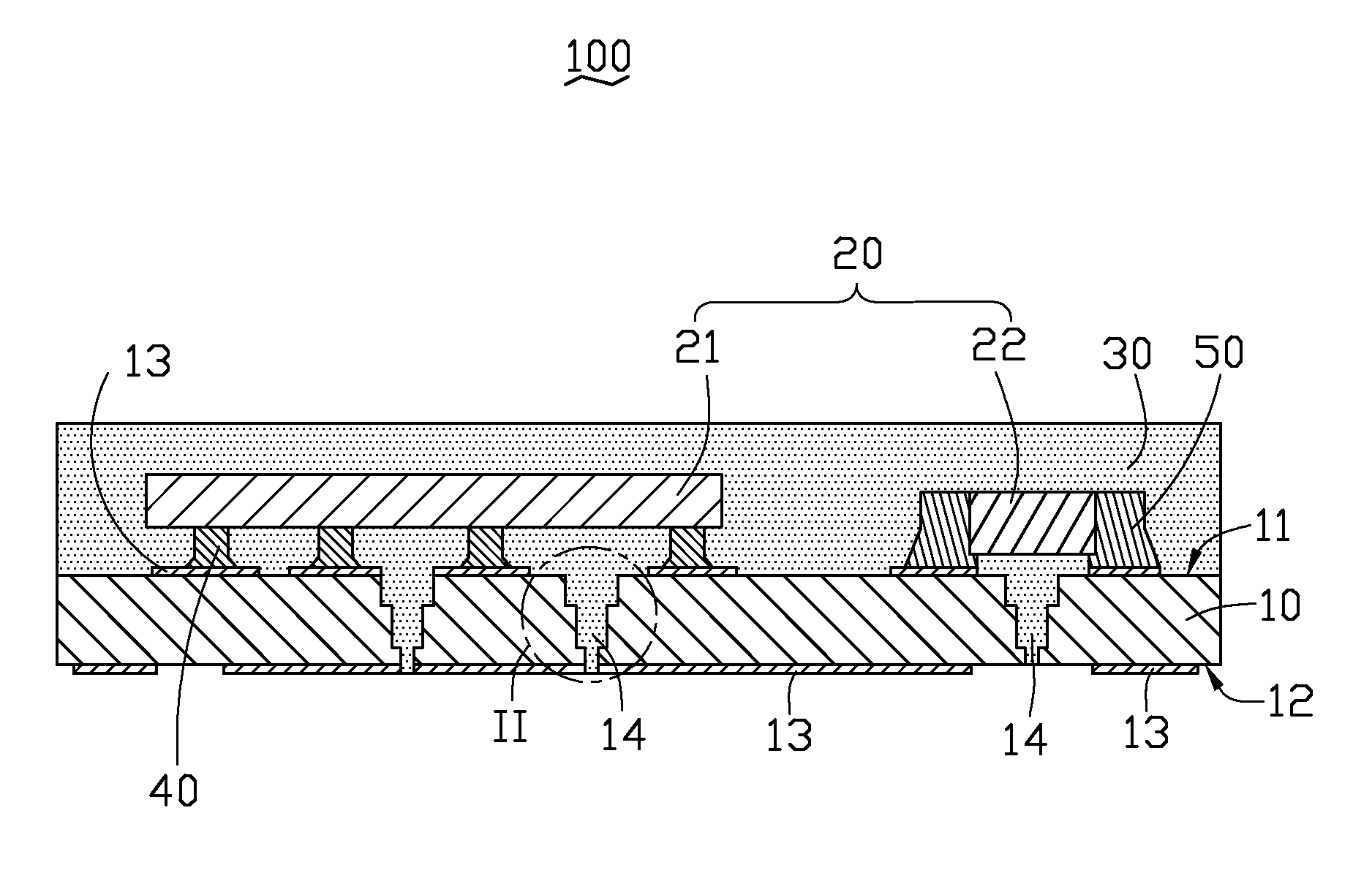
[0012]With reference to FIG. 1, a package assembly 100 includes a substrate 10, a plurality of electronic components 20 on a top surface 11 of the substrate 10 and electrically connected to the substrate 10, a encapsulation body 30 encapsulating the electronic components 20 with the substrate 10. The top surface 11 and a bottom surface 12 opposite to the top surface 11 includes a plurality of solder pads 13. The plurality of electronic components 20 are electrically connected to the substrate 10 via the plurality of solder pads 13. In the embodiment, the electronic components 20 may include a chip 21 (e.g., an integrated circuit, or a microproces...


PUM


Abstract

A package assembly includes a substrate, an electronic component, and an encapsulation body. The electronic component is located on the substrate and electrically connected to the substrate. The encapsulation body encapsulates the electronic component with the substrate. A portion of the substrate corresponding to the electronic component defines a plurality of through holes. A diameter of each of the plurality of through holes gradually reduces from a top surface of the substrate toward a bottom surface of the substrate. The plurality of through holes prevent melting remnants of the encapsulation body from flowing outside of the substrate.

Description

BACKGROUND[0001]1. Technical Field[0002]The present disclosure generally relates to package assemblies and methods for manufacturing the same, and more particularly to a package assembly with a plurality of through holes on a substrate.[0003]2. Description of Related Art[0004]Generally, a package assembly defines a plurality of through holes on a portion of substrate to dissipate heat, and the portion usually corresponds to large grounding pads. The plurality of through holes are filled with filling materials. However, if a large sized electronic component, such as a flip-flow chip, is packed on the substrate, air between the electronic component and the substrate is not easy to escape from the through holes, due to the filling materials filled in the plurality of through holes. As a results, cavities are unfortunately formed between the electronic component and the substrate, which leads to a weak performance of the package assembly.BRIEF DESCRIPTION OF THE DRAWINGS[0005]Many aspec...

Claims


Application Information

Patent Timeline
Patent Type & Authority Patents(United States)
IPC IPC(8): H01L23/52H01L21/56H01L23/13H01L23/31H01L23/498
CPCH01L23/49827H01L21/56H01L23/3121H01L21/563H01L23/13H01L21/565H01L23/3142H01L2224/16245H01L2224/16225H01L2924/16151H01L2924/19105
Inventor YANG, WANG-LAI
Owner SHUNSIN TECH (ZHONG SHAN) LTD
Why Eureka
Try Eureka