
DFB laser diode having a lateral coupling for large output power

a laser diode and lateral coupling technology, which is applied in the direction of lasers, electrical equipment, laser details, etc., can solve the problems of affecting the quality of the layers that form the laser diode, the coupling constant is reduced, and the production process is complex, so as to reduce the maximum intensity density, reduce the coupling constant, and reduce the quality of other parameters

Active Publication Date: 2014-10-07
NANOPLUS GMBH
View PDF18 Cites 4 Cited by
  • Summary
  • Abstract
  • Description
  • Claims
  • Application Information

AI Technical Summary

Benefits of technology

[0022]Due to the thick wave guide layer, the spatial distribution of the optical intensity in this layer and therefore perpendicular to the stack of layers can extend over a larger distance. This broadening of the laser radiation in a transverse direction results in a reduction of the maximum of the optical intensity by having equal optical power within the laser mode. Thus, by having the same optical power of the laser mode, the maximum optical power density on the laser mirror and thus also its load is reduced. Thus, for a given maximum load of the laser mirror, the light output that can be coupled out from the laser cavity can be increased. Moreover, the broader distribution of the radiation of the laser mode in direction of the stack of layers of the laser cavity leads to a reduced transverse divergence angle of the laser light after emission of the laser cavity. Due to this reduced beam divergence in transverse direction which is similar to the divergence angle in lateral direction, a simpler yet more efficient coupling of the laser radiation into optical elements is achieved.
[0026]For DFB laser diodes having a lateral coupling, a thick wave guide layer above the active layer essentially leads to coupling out of the emitted laser radiation by reducing the spatial overlapping with the periodic surface structure. Thereby, the effect of the distributed feedback and thus the suppression of further natural modes of the laser cavity within the amplification bandwidth can be clearly reduced. Due to the combination of a thin wave guide layer above and a thick wave guide layer below the active layer, a reduction of the coupling factor of the periodic surface structure can widely be avoided. At the same time the propagation of the optical intensity in transverse direction is increased due to this layer combination as compared to conventional layer design according to prior art. This leads to a smaller far field angle in transverse direction. This leads to a higher degree of efficiency when the laser radiation is coupled into rotation-symmetric lenses, which results in an increased amount of available or useable optical power by having the same light output emitted by the laser diode.
[0031]By tapering the ridge into the direction of one laser mirror, the intensity distribution of the laser mode is shifted downwards into the direction of the lower wave guide layer. In particular for a thick lower wave guide layer this leads at the same time to a broadening of the optical intensity distribution at the laser mirror within the lower wave guide layer. Linked thereto is a reduction of the maximum intensity density at the laser mirror which again may be used for increasing the light output that can be coupled out from the laser cavity using the laser mirror. Moreover, the broadening of the transverse intensity distribution that is caused by the tapering results in a reduction of the divergence angle of the light output that is emitted from the laser cavity into transverse direction. Thereby, it can be achieved that the transverse and lateral divergence angle are nearly equal to each other. Thus, by tapering the ridge the coupling of laser radiation in a simple yet efficient manner becomes possible.
[0039]An additional layer with a large refractive index and that is embedded within the ridge results in a deformation of the optical intensity distribution within this layer and into the direction of this layer. The modified transverse intensity distribution changes the coupling strength of the laser mode on the periodic surface structure that is arranged on the upper wave guide layer. Thereby, it is possible to compensate—at least partially—a reduced coupling constant between the laser mode and the periodic surface structure that is caused by the broadened upper wave guide layer. The layer embedded within the ridge has a large refractive index and thus provides a further degree of freedom in order to reduce the maximum intensity density on the laser mirror without significantly reducing the quality of other parameters of the laser.

Problems solved by technology

This interruption of the layer growth, however, has some problems: On the one hand, this production process is complex and on the other hand, the quality of the layers that form the laser diode may be compromised by the structuring process and the second epitaxial process due to the introduction of crystal defects.
This may have negative effects on the efficiency and in particular on the lifetime of the DFB laser diodes.
Due to the production of DFB laser diodes having a lateral coupling in a single epitaxial process, the crystal quality of the stack of layers that forms the laser diode cannot be influenced by interrupting the growth of the layer, the structuring process and the second epitaxial process.
In connection with the precisely adjustable emission wavelength this results in a large yield in the production process.
Due to their distributed feedback mechanism, DFB laser diodes usually comprise rather low output power.
However, some applications require the allocation of large light output which cannot be provided by DFB laser diodes having a lateral coupling that have been produced according to prior art.
These degradation processes result in a sudden destruction of the laser mirror due to a local melting of the semiconductor material.
This process is referred to as catastrophic optical damage or COD.

Method used


Image

  • DFB laser diode having a lateral coupling for large output power
  • DFB laser diode having a lateral coupling for large output power
  • DFB laser diode having a lateral coupling for large output power

Examples


Embodiment Construction

[0067]In the following, preferred embodiments of the apparatuses according to the present invention are described in more detail.

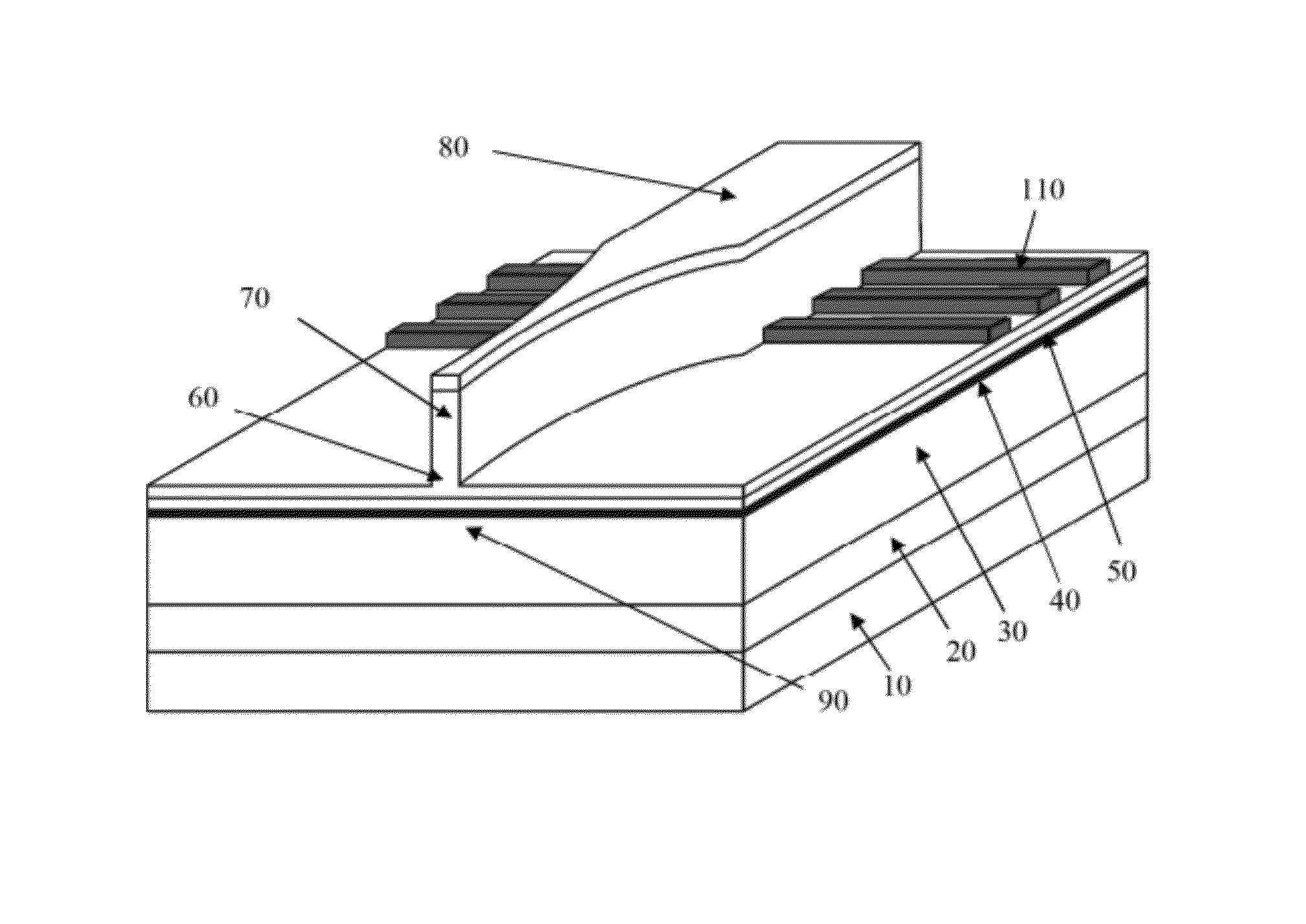
[0068]FIG. 1 schematically illustrates the most important layers that represent a DFB laser diode having a lateral coupling. The different layers are deposited on a semiconductor substrate 10 using an epitaxial process. The material system of semiconductor substrate 10 is defined by the desired wave length of the laser diode. The principles underlying the present invention that are explained in detail in the following, can be applied to all known material systems in order to manufacture laser diodes that emit light from the blue (e.g., gallium nitride substrates) to the deep infrared wave length range (e.g., based on gallium antimonide substrates). Besides substrates on the basis of III / V compound semiconductors, the disclosed principles can also be applied to DFB laser diodes with lateral coupling that are based on II / VI semiconductor substrates or other ...


PUM


Abstract

The invention relates to a DFB laser diode having a lateral coupling, which comprises at least one semi-conductor substrate (10), at least one active layer (40) that is arranged on the semiconductor substrate, at least one ridge (70) that is arranged above the active layer (40), at least one periodic surface structure (110) that is arranged next to the ridge (70) above the active layer (40) and at least one wave guide layer (30, 50) comprising a thickness ≧1 μm that is arranged below and / or above the active layer.

Description

1. TECHNICAL FIELD[0001]The present invention relates to a DFB laser diode having a lateral coupling for large output power.2. PRIOR ART[0002]Laser diodes can be used as coherent light sources and play an important part in many economic areas. As an example two areas of application are illustrated: The use for data transmission in telecommunications and as analysis tool in the field of sensor technology. In these as well as in most other areas of application it is very important that the radiation emitted by the laser diode essentially corresponds to a single natural mode of the laser cavity and that the bandwidth of this single natural mode is small.[0003]Semiconductor lasers usually emit light of several natural modes which is due to their broad amplification spectrum. In order to ensure that the emitted laser radiation essentially comprises light of a single natural mode, the concept of distributed feedback (DFB) of the laser light between both mirrors of the laser cavity has bee...

Claims


Application Information

Patent Timeline
Patent Type & Authority Patents(United States)
IPC IPC(8): H01S5/00H01S5/10H01S5/12H01S5/20H01S5/22
CPCH01S5/1228H01S5/1014H01S5/1203H01S5/1237H01S5/22H01S5/2004H01S5/2031
Inventor KOETH, JOHANNES BERNHARDZELLER, WOLFGANG
Owner NANOPLUS GMBH
Learn More