
Method of operating semiconductor device

a technology of semiconductor devices and operating methods, applied in the direction of static storage, digital storage, instruments, etc., can solve the problems of reducing the reliability of the semiconductor device and the reliability of the program operation

Active Publication Date: 2014-10-07
SK HYNIX INC
View PDF11 Cites 8 Cited by
  • Summary
  • Abstract
  • Description
  • Claims
  • Application Information

AI Technical Summary

Benefits of technology

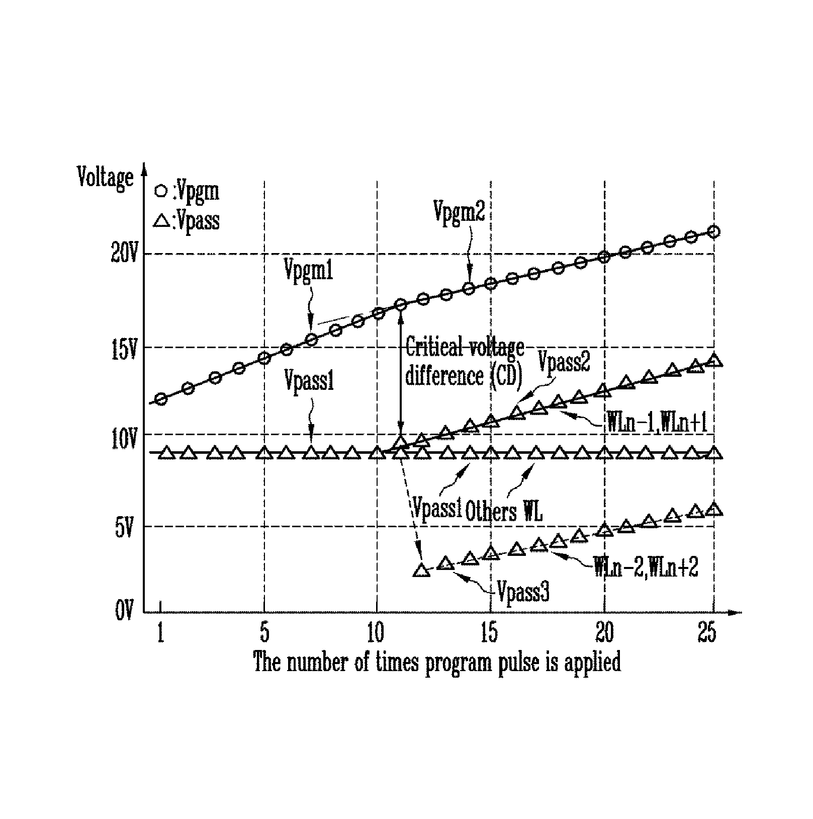
[0015]Various embodiments relate to preventing unselected memory cells adjacent to a selected memory cell from being erased by not allowing the voltage difference between a program voltage and a pass voltage to exceed a critical voltage difference during a program operation.
[0016]Various embodiments relate to avoiding leakage that may occur in a selected memory cell and suppressing interference between adjacent memory cells by reducing the rate of increase of a program voltage after the program voltage being gradually increased reaches a predetermined level.

Problems solved by technology

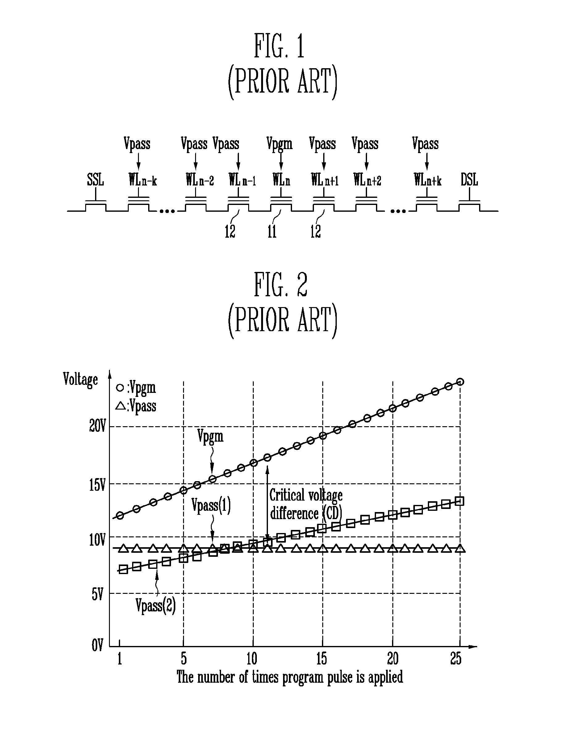
Additionally, as for unselected memory cells having completed the program operation among the unselected memory cells 12 adjacent to the selected memory cell 11, in the case that threshold voltages of these memory cells decrease, other data may be inadvertently read during a read operation subsequent to the program operation, which may reduce the reliability of the semiconductor device.
In other words, after the program voltage Vpgm being applied to the selected word line WLn gradually increases during the program operation in order for the voltage difference between the program voltage Vpgm and the pass voltage Vpass to reach the critical voltage difference CD, the threshold voltage of the selected memory cell and the threshold voltages of the neighboring memory cells may change, and leakage of the neighboring memory cells may be generated, which may lead to reduction in reliability of the program operation.

Method used


Image

  • Method of operating semiconductor device
  • Method of operating semiconductor device
  • Method of operating semiconductor device

Examples


first embodiment

[0051]FIG. 4 is a graph illustrating a program method according to the present invention.

[0052]Referring to FIGS. 3 and 4, a program operation is performed by an Incremental Step Pulse Program (ISPP) method where the program voltage Vpgm is gradually increased. During a program operation, a program enable voltage, e.g. a ground voltage, is applied to bit lines coupled to selected cell strings, while a program inhibit voltage, e.g. a power voltage, is applied to bit lines coupled to unselected cell strings. While the program enable voltage or the program inhibit voltage is applied to the bit lines, a first program voltage Vpgm1 that is increased if necessary by a first step voltage is applied to the selected word line WLn, whereas the pass voltage is applied to unselected word lines WLn−1 to WLn−k and WLn+1 to WLn+k.

[0053]At the initial stage of the program operation using the ISPP method, the voltage difference between the first program voltage Vpgm1 and a first pass voltage Vpass1 ...

second embodiment

[0059]FIG. 5 is a graph illustrating a program method according to the present invention.

[0060]Referring to FIGS. 3 and 5, a program operation is performed by an Incremental Step Pulse Program (ISPP) method where a program voltage is gradually increased. During a program operation, a program enable voltage, e.g. a ground voltage, is applied to bit lines coupled to selected cell strings, while a program inhibit voltage, e.g. a power voltage, is applied to bit lines coupled to unselected cell strings. While the program enable voltage or the program inhibit voltage is applied to the bit lines, the first program voltage Vpgm1 that is increased if necessary by a first step voltage is applied to the selected word line WLn, whereas the pass voltage is applied to the unselected word lines WLn−1 to WLn−k and WLn+1 to WLn+k.

[0061]At the initial stage of the program operation, the voltage difference between the first program voltage Vpgm1 and the first pass voltage Vpass1 is smaller than the c...

eighth embodiment

[0118]FIG. 11 is a graph illustrating a program method according to the present invention.

[0119]Referring to FIGS. 3 and 11, a program operation is performed by an Incremental Step Pulse Program (ISPP) method where a program voltage is gradually increased. During a program operation, a program enable voltage, e.g. a ground voltage is applied to bit lines coupled to selected cell strings, while a program inhibit voltage, e.g. a power voltage, is applied to bit lines coupled to unselected cell strings. While the program enable voltage or the program inhibit voltage is applied to the bit lines, the first program voltage Vpgm1 that is increased if necessary by a first step voltage is applied to the selected word line WLn, whereas the eleventh pass voltage Vpass11 being gradually increased is applied to the unselected word lines WLn−1 to WLn−k and WLn+1 to WLn+k. The eleventh pass voltage Vpass11 has a rate of increase lower than the first program voltage Vpgm1.

[0120]The eleventh pass vo...


PUM


Abstract

A semiconductor device is operated by, inter alia: programming selected memory cells by applying a first program voltage which is increased by a first step voltage to a selected word line and by applying a first pass voltage having a constant level to unselected word lines, and when a voltage difference between the first program voltage and the first pass voltage reaches a predetermined voltage difference, programming the selected memory cells by applying a second program voltage which is increased by a second step voltage lower than the first step voltage to the selected word line and by applying a second pass voltage which is increased in proportion to the second program voltage to first unselected word lines adjacent to the selected word line among the unselected word lines.

Description

CROSS-REFERENCE TO RELATED APPLICATION[0001]This application claims priority to and the benefit of Korean patent application numbers 10-2011-0067013 filed on Jul. 6, 2011 and 10-2012-0068544 filed on Jun. 26, 2012, the entire disclosure of which is incorporated herein by reference in its entirety.BACKGROUND[0002]1. Field of Invention[0003]Various embodiments of the present invention relate generally to a method of operating a semiconductor device and, more particularly, to a program method.[0004]2. Description of Related Art[0005]A semiconductor device includes a memory cell array that stores data therein. The memory cell array consists of a plurality of cell blocks, each of which includes a plurality of cell strings. The cell strings have the same structure as each other, and are described below in more detail.[0006]FIG. 1 is a circuit diagram illustrating a cell string.[0007]With reference to FIG. 1, the cell string includes a drain select transistor, a plurality of memory cells, ...

Claims


Application Information

Patent Timeline
Patent Type & Authority Patents(United States)
IPC IPC(8): G11C16/10
CPCG11C16/10G11C16/0483G11C16/08G11C16/3427
Inventor ARITOME, SEIICHI
Owner SK HYNIX INC
Learn More