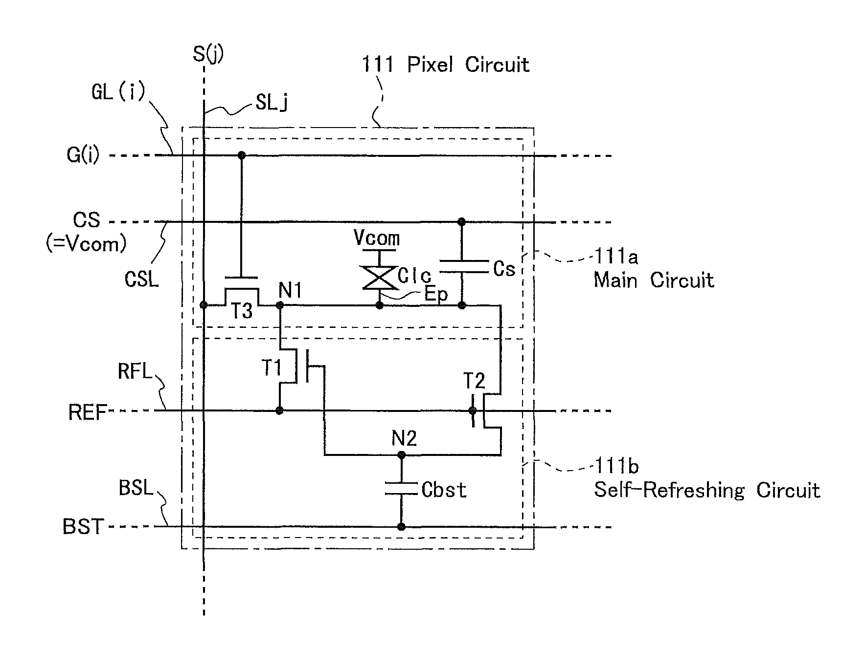
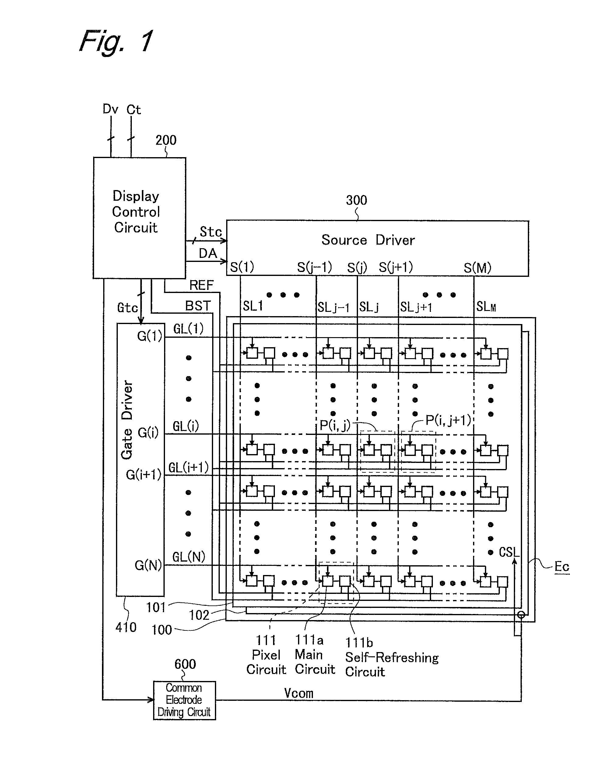
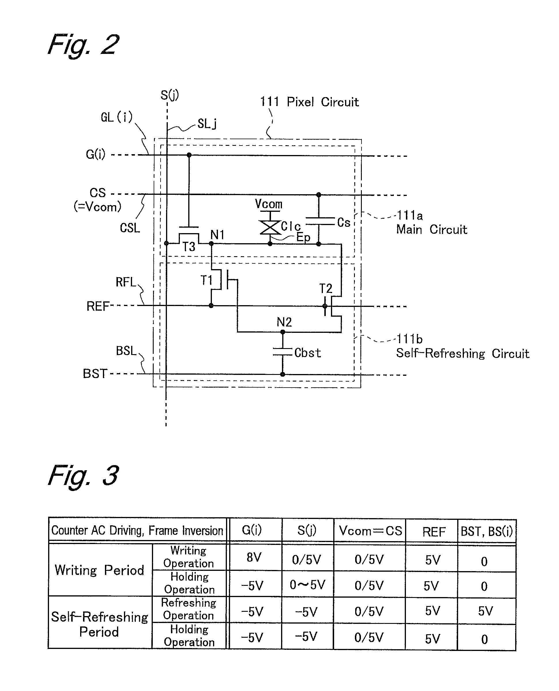
[0137]According to the fifteenth aspect of the present invention, a voltage pulse is applied simultaneously to all of the second wirings in the first operation mode. Therefore, a refreshing operation, i.e. voltage supply from the first wiring to the predetermined electrode by the first active element in accordance with a voltage value of the predetermined electrode, takes place collectively for all of the pixel circuits. The arrangement makes it possible to generate the voltage pulse for the refreshing operation with a simple configuration.
[0138]According to the sixteenth aspect of the present invention, a voltage pulse is applied selectively to the second wirings in batch per scanning signal line, in the first operation mode. Therefore, a refreshing operation, i.e. voltage supply from the first wiring to the predetermined electrode by the first active element in accordance with a voltage value of the predetermined electrode, takes place in batch of the pixel circuits belonging to one scanning signal line as a unit. For this reason, the arrangement decreases peak current due to the refreshing operation in comparison to the collective refreshing described above.
[0143]According to the twenty-first aspect of the present invention, the voltage to be supplied from the data signal line to the predetermined electrode in order to make the capacitance in the pixel circuit hold pixel data lies within a range of 0 volt to a predetermined positive voltage value. In the first operation mode, the above off-resistance-division voltage is set to a voltage value (the predetermined voltage) which is approximately equal to the lowest of the voltages to be supplied to the predetermined electrode. Therefore, the arrangement makes it possible to maintain the voltage of the predetermined electrode closely to the voltage which was supplied from data signal line to the predetermined electrode, by supplying a voltage(s) which are not the lowest of those voltages to be supplied to the predetermined electrode from the first wiring, and supplying the lowest (voltage approximately equal thereto) of the voltages from a connection point between the first active element and the third active element, in the first operation mode.
[0140]According to the eighteenth aspect of the present invention, if the predetermined electrode is supplied with a voltage which lies within a predetermined range set around a reference voltage given by the first wiring, the first active element is turned ON when the voltage pulse is applied to the second wiring, to supply the predetermined electrode with the voltage of the first wiring. On the other hand, if the voltage pulse is not applied to the second wiring or if the predetermined electrode is supplied with a voltage which lies out of the above-mentioned predetermined range but lies within a different predetermined range, the first active element is turned OFF, and therefore, the voltage of the first wiring is not supplied to the predetermined electrode, so there is no voltage change in the predetermined electrode.
[0141]According to the nineteenth aspect of the present invention, the voltage of each data signal line is fixed to a predetermined value in the first operation mode. This suppresses operation by the data signal line driving circuit, keeping output buffers and other components in the data signal line driving circuit to stay in a deactivated state, leading to remarkable reduction in power consumed by the display device.
[0143]According to the twenty-first aspect of the present invention, the voltage to be supplied from the data signal line to the predetermined electrode in order to make the capacitance in the pixel circuit hold pixel data lies within a range of 0 volt to a predetermined positive voltage value. In the first operation mode, the above off-resistance-division voltage is set to a voltage value (the predetermined voltage) which is approximately equal to the lowest of the voltages to be supplied to the predetermined electrode. Therefore, the arrangement makes it possible to maintain the voltage of the predetermined electrode closely to the voltage which was supplied from data signal line to the predetermined electrode, by supplying a voltage(s) which are not the lowest of those voltages to be supplied to the predetermined electrode from the first wiring, and supplying the lowest (voltage approximately equal thereto) of the voltages from a connection point between the first active element and the third active element, in the first operation mode.
[0144]According to the twenty-second aspect of the present invention, the off-resistance-division voltage approximately equals to zero, in the first operation mode. Therefore, the arrangement makes it possible to maintain the voltage of the predetermined electrode closely to the voltage which was supplied from data signal line to the predetermined electrode, by supplying a non-near-zero voltage(s) of the voltages to be supplied to the predetermined electrode from the first wiring, and supplying the voltage which is approximately zero volt from a connection point between the first active element and the third active element, in the first operation mode.
[0145]According to the twenty-third aspect of the present invention, in the second operation mode, data signal is supplied to the predetermined electrode via the data signal line and the third active element whereby data is written from the data signal line to the pixel circuit when the third active element is in ON state.
[0146]According to the twenty-fourth aspect of the present invention, the second active element is in ON state, so the control terminal of the first active element is supplied with the voltage of the predetermined electrode, which prevents the first active element from turning ON. Thus, the pixel circuit operates in a conventional manner, and data signal is supplied from the data signal line to the predetermined electrode.
[0147]According to the twenty-fifth aspect of the present invention, the second active element is in OFF state in the second operation mode. Thus, by setting the control terminal voltage of the first active element not to turned ON regardless of the voltage of the predetermined electrode, it becomes possible to let the pixel circuit operate in a conventional manner to supply data signal from the data signal line to the predetermined electrode.
[0148]According to the twenty-sixth aspect of the present invention, in the third operation mode, a voltage of inverted polarity is supplied to the predetermined electrode via the data signal line so that the voltage to be applied to the capacitance to hold pixel data will have an inverted polarity. Therefore, the arrangement provides image display by AC drive, for example in order to prevent display quality of liquid crystal display devices from being reduced due to ion accumulation on the electrode side, premature deterioration of the liquid crystal, etc. which are caused by DC voltage application to the liquid crystal.
[0153]In whichever of the thirty-second and the thirty-third aspects of the present invention, the predetermined electrode for formation of the capacitance for holding pixel data is capacitance-coupled with the third wiring. Therefore, by supplying the third wiring with a predetermined voltage, the arrangement makes it possible to stably hold the voltage captured as pixel data in the pixel circuit from the data signal line.
[0150]According to the twenty-eighth aspect of the present invention, the time interval for the polarity inversion in the third operation mode is longer than ten times the time interval for voltage pulse application to the second wiring in the first operation mode. This makes it possible to drastically reduce occasions for driving data signal lines and other components to perform polarity inversion while suppressing voltage creep in the predetermined electrode caused by leak current. As a result, it is now possible to make sufficient reduction of power consumption in displaying (permanent display of) still images while avoiding poor display quality caused by flickering or decreased contrast.
[0153]In whichever of the thirty-second and the thirty-third aspects of the present invention, the predetermined electrode for formation of the capacitance for holding pixel data is capacitance-coupled with the third wiring. Therefore, by supplying the third wiring with a predetermined voltage, the arrangement makes it possible to stably hold the voltage captured as pixel data in the pixel circuit from the data signal line.
[0153]In whichever of the thirty-second and the thirty-third aspects of the present invention, the predetermined electrode for formation of the capacitance for holding pixel data is capacitance-coupled with the third wiring. Therefore, by supplying the third wiring with a predetermined voltage, the arrangement makes it possible to stably hold the voltage captured as pixel data in the pixel circuit from the data signal line.
[0153]In whichever of the thirty-second and the thirty-third aspects of the present invention, the predetermined electrode for formation of the capacitance for holding pixel data is capacitance-coupled with the third wiring. Therefore, by supplying the third wiring with a predetermined voltage, the arrangement makes it possible to stably hold the voltage captured as pixel data in the pixel circuit from the data signal line.


