Reverse-conducting power semiconductor device

a reverse-conducting, semiconductor technology, applied in semiconductor devices, diodes, electrical devices, etc., can solve problems such as overheating

Active Publication Date: 2014-09-30
HITACHI ENERGY LTD
View PDF6 Cites 3 Cited by
  • Summary
  • Abstract
  • Description
  • Claims
  • Application Information

AI Technical Summary

Benefits of technology

[0032]The inventive reverse conducting power semiconductor device has a better thermal resistance, because due to the distributed diode and IGCT cells the heat is distributed over a greater area. In case of the device working in IGCT mode exemplarily, due to the distributed cells, the heat can easily spread also into the diode cells and therefore, the temperature within the device is lower than for a known device, in which the single diode is concentrated to one continuous area so that the heat spreads much less efficient into the diode area.
[0033]Also the current handling capability is better than the known devices due to the at least part or full integration of the diode and IGCT structures for allowing part or full utilization of the wafer area (exemplarily made of silicon) in IGCT mode and sufficient utilization of the wafer area in the diode mode of operation. The above effect is reached due to the close proximity of the IGCT and diode cells, e.g., the alternating arrangement of IGCT and diode cells, which would allow the charge plasma during conduction for the IGCTs to spread laterally into or through the adjacent diode cells. Depending on the size of the diode cells the holes enter the diode cells (holes flow into the second anode layer) and can even pass through them.

Problems solved by technology

This might lead to overheating problems.

Method used


Image

  • Reverse-conducting power semiconductor device
  • Reverse-conducting power semiconductor device
  • Reverse-conducting power semiconductor device

Examples


Embodiment Construction

[0025]Exemplary embodiments of the present disclosure provide a reverse conducting power semiconductor device with improved performance of the device in view of thermal and electrical properties and reduced size.

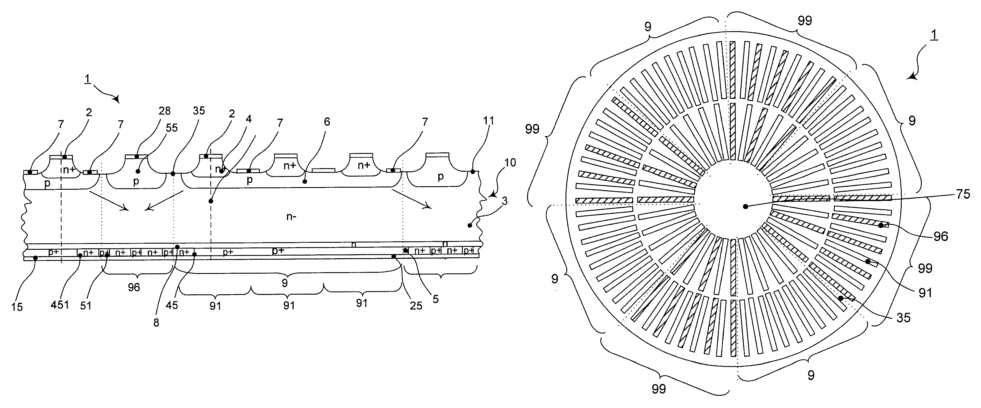
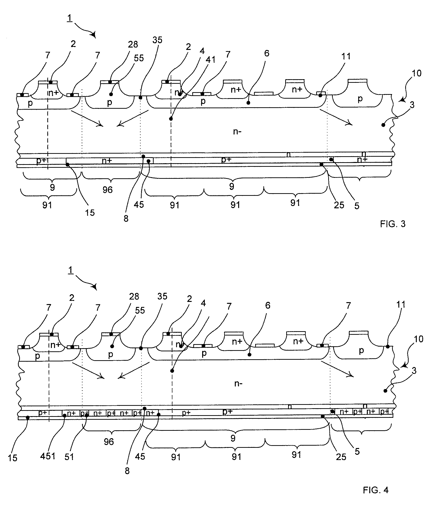
[0026]An exemplary reverse conducting power semiconductor device disclosed herein can include a wafer having a first main side and a second main side, which is arranged parallel to the first main side. The device can also include a plurality of diode cells and a plurality of IGCT cells (integrated gate commutated thyristor cells), wherein each IGCT cell has (e.g., comprises) layers in the following order between the first and second main side a cathode electrode, a first cathode layer of the first conductivity type, a base layer of the second conductivity type, a drift layer of the first conductivity type, a buffer layer of the first conductivity type, a first anode layer of the second conductivity type, and a first anode electrode.

[0027]Each IGCT cell further includes a gat...


PUM


Abstract

An exemplary reverse-conducting power semiconductor device with a wafer having a first main side and a second main side parallel to the first main side. The device includes a plurality of diode cells and a plurality of IGCT cells, each IGCT cell including between the first and second main side: a first anode electrode, a first anode layer of a first conductivity type on the first anode electrode, a buffer layer of a second conductivity type on the first anode layer, a drift layer of the second conductivity type on the buffer layer, a base layer of the first conductivity type on the drift layer, a first cathode layer of a second conductivity type on the base layer, and a cathode electrode on the first cathode layer. A mixed part includes the second anode layers of the diode cells alternating with the first cathode layers of the IGCT cells.

Description

RELATED APPLICATION(S)[0001]This application is a continuation under 35 U.S.C. §120 of International application PCT / EP2011 / 066979 filed Sep. 29, 2011, designating the U.S. and claiming priority to European application EP 10181546.2 filed Sep. 29, 2010. The content of each prior application is hereby incorporated by reference in its entirety.FIELD[0002]The disclosure relates to the field of power semiconductor devices, and particularly to a reverse conducting power semiconductor device.BACKGROUND INFORMATION[0003]As shown in FIG. 1, the RC-IGCT 100 includes within one wafer 10 an integrated gate commutated thyristor (IGCT) part 9 with IGCT cells 91 and a single built-in free-wheeling diode 97.[0004]FIG. 2 shows a cut through an RC-IGCT according to a known implementation. The reverse-conducting semiconductor device 100 also includes a wafer 10 with layers of different conductivity types between a first main side 11, which is the cathode side of the integrated IGCT, and a second main...

Claims


Application Information

Patent Timeline
Patent Type & Authority Patents(United States)
IPC IPC(8): H01L29/66H01L21/332
CPCH01L29/747H01L29/0692H01L29/0834H01L29/7416H01L29/7428H01L29/744H01L29/74
Inventor RAHIMO, MUNAFARNOLD, MARTINSTIASNY, THOMAS
Owner HITACHI ENERGY LTD
Why Eureka
Try Eureka