
Vertical light-emitting diode

a light-emitting diode and vertical technology, applied in the direction of basic electric elements, electrical equipment, semiconductor devices, etc., can solve the problems of low thermal conductivity, low reliability of light-emitting devices, current blockage, etc., to improve the reliability of vertical light-emitting diodes and short circuit protection

Active Publication Date: 2014-02-18
QUANZHOU SANAN SEMICON TECH CO LTD
View PDF3 Cites 0 Cited by
  • Summary
  • Abstract
  • Description
  • Claims
  • Application Information

AI Technical Summary

Benefits of technology

[0005]To solve the problems in the prior art that the vertical light-emitting diode may lose short circuit protection and the resulting decreased reliability because the SiO2 insulating film is easy to split or fall off, the present invention provides a new vertical light-emitting diode with a short circuit protection function.
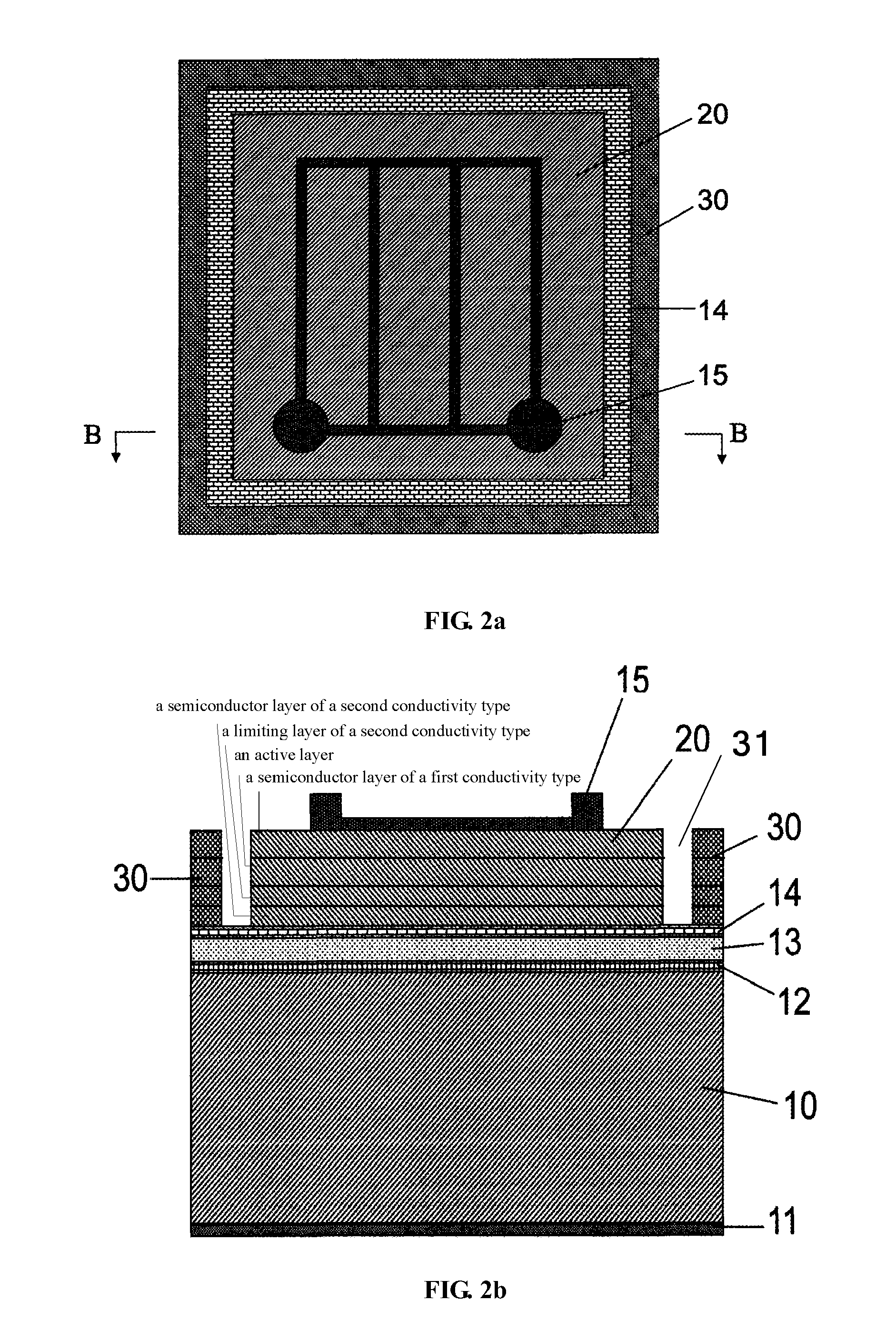
[0015]The barrier for the semiconductor light-emitting layer is an innovation by the present invention. The barrier for the semiconductor light-emitting layer may be formed by removing a portion of a semiconductor light-emitting layer through etching to generate an isolation trench. The barrier for the semiconductor light-emitting layer surrounds the semiconductor light-emitting layer, and can effectively prevent the metal particles in chip dicing and the conductive adhesive in packaging from reaching the semiconductor light-emitting layer, thereby providing short circuit protection for the semiconductor light-emitting layer and improving the reliability of the vertical light-emitting diode according to the present invention.
[0017]The present invention has the advantages that: the barrier for the semiconductor light-emitting layer surrounds the semiconductor light-emitting layer with a distance therebetween, and can effectively prevent the metal particles in chip dicing and the conductive adhesive in packaging from reaching the semiconductor light-emitting layer, thereby providing short circuit protection for the semiconductor light-emitting layer and improving the reliability of the vertical light-emitting diode according to the present invention.

Problems solved by technology

The lateral current paths through the n-GaN layer are different in length, resulting in current blocking and decreased light-emitting device reliability.
Sapphire also has a low thermal conductivity, which may limit the light-emission power and efficiency of the GaN-based light-emitting devices.
Therefore, for example, in the process of chip dicing, generated metal particles may be splashed to the sidewall of the quantum well light-emitting layer, causing electricity leakage and ineffectiveness of the light-emitting diode; in the process of packaging, the conductive adhesive may extend to the light-emitting layer, causing electricity leakage and ineffectiveness of the light-emitting diode; and in the process of chip handling, the light-emitting layer may be damaged, also causing electricity leakage.
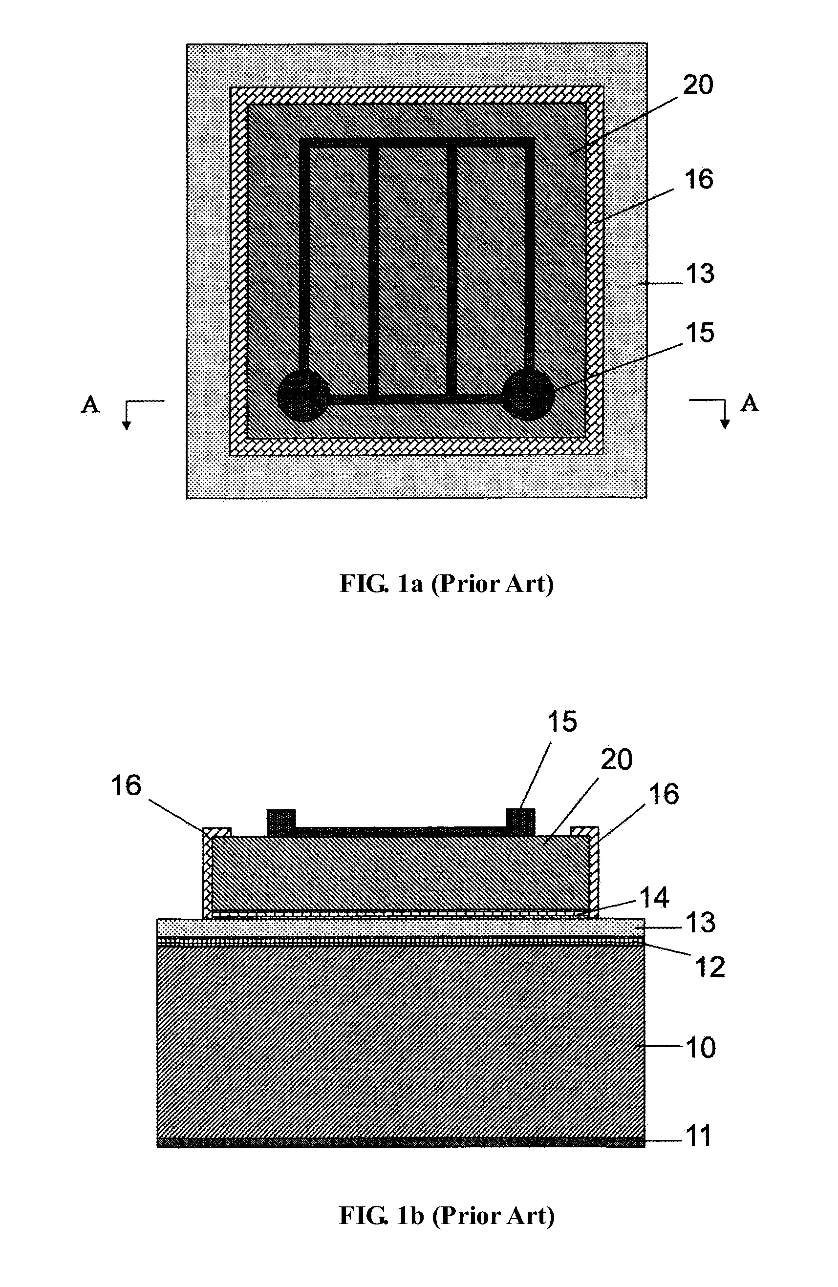
The vertical light-emitting diode in the prior art is characterized in that: short circuit protection is based on the electrical insulating material e.g. SiO2, SiN or Al2O3; however it has the drawbacks that: the insulating film of e.g. SiO2 is normally formed on the surface and sidewall of the semiconductor light-emitting layer by plasma-enhanced chemical vapor deposition (PECVD) at a certain temperature, due to the large stress inside the deposited SiO2 film and its poor adhesiveness to the semiconductor light-emitting layer, the SiO2 film may easily split or fall off, failing the purpose of short circuit protection.

Method used


Image

  • Vertical light-emitting diode
  • Vertical light-emitting diode
  • Vertical light-emitting diode

Examples


Embodiment Construction

[0028]The present invention will be further described hereinafter in conjunction with the accompanying drawings and the embodiments.

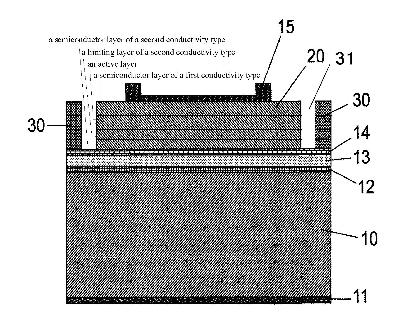
[0029]FIG. 2a and FIG. 2b illustrate a vertical light-emitting diode with a short circuit protection function. A first electrode 11 is formed on a bottom of a heat dissipation substrate 10 made of GaAs. A second electrode 12 is formed on the heat dissipation substrate 10. A third electrode 14 is formed on the welding metal layer 13. A semiconductor light-emitting layer 20 is formed on the third electrode 14. The welding metal layer 13 is formed on the second electrode 12. The semiconductor light-emitting layer 20 is formed at a central region on the third electrode 14. The semiconductor light-emitting layer 20 includes: an n-type conductive layer made of GaN, an active layer made of InGaN, a p-type limiting layer made of AlGaN, and a p-type conductive layer made of GaN. The semiconductor light-emitting layer 20 provides the light emitting function. A fo...


PUM


Abstract

A vertical light-emitting diode with a short circuit protection function includes a heat dissipation substrate, a second electrode, a welding metal layer and a third electrode; a semiconductor light-emitting layer formed on the third electrode; a barrier for the semiconductor light-emitting layer with an isolation trench, so that the barrier for the semiconductor light-emitting layer surrounds the semiconductor light-emitting layer on a central region of the third electrode, with the isolation trench therebetween. The barrier for the semiconductor light-emitting layer has a structure the same as the semiconductor light-emitting layer, and the isolation trench exposes the third electrode. A fourth electrode is formed on the semiconductor light-emitting layer. The barrier prevents the metal particles in chip dicing and the conductive adhesive in packaging from reaching the semiconductor light-emitting layer, thereby providing short circuit protection and improving the reliability of the vertical light-emitting diode.

Description

FIELD OF INVENTION[0001]The present invention relates to a vertical light-emitting diode, and particularly to a vertical light-emitting diode with a short circuit protection function.BACKGROUND OF THE INVENTION[0002]Nowadays, most of the GaN-based light-emitting diodes have an epitaxial layer grown on a sapphire substrate. Sapphire has a low electrical conductivity, and the GaN-based light-emitting devices normally have a lateral structure in which both electrodes are on the same side of the device. The lateral current paths through the n-GaN layer are different in length, resulting in current blocking and decreased light-emitting device reliability. Sapphire also has a low thermal conductivity, which may limit the light-emission power and efficiency of the GaN-based light-emitting devices. Consequently, problems concerning heat dissipation, light emission and static electricity reducing can be solved by removing the sapphire substrate and forming the light-emitting devices with a v...

Claims


Application Information

Patent Timeline
Patent Type & Authority Patents(United States)
IPC IPC(8): H01L33/00
CPCH01L33/20H01L33/647H01L33/38H01L33/641H01L33/387
Inventor LIN, XUEJIAOHUANG, HUIJUN
Owner QUANZHOU SANAN SEMICON TECH CO LTD
Learn More