
Liquid crystal display array substrate and method for manufacturing the same

a technology of liquid crystal display and array substrate, which is applied in the field of liquid crystal display, can solve the problems of difficult repair of open circuit failure and reduction of viewing angle characteristics of liquid crystal display

Active Publication Date: 2014-02-18
LG DISPLAY CO LTD
View PDF8 Cites 0 Cited by
  • Summary
  • Abstract
  • Description
  • Claims
  • Application Information

AI Technical Summary

Benefits of technology

The invention provides a way to make a liquid crystal display that can repair any problems that might occur with the data lines. This means that the display can be used for longer periods of time without malfunctions.

Problems solved by technology

However, the drive of the liquid crystals by the vertical electric field results in a reduction in viewing angle characteristics of the liquid crystal display.
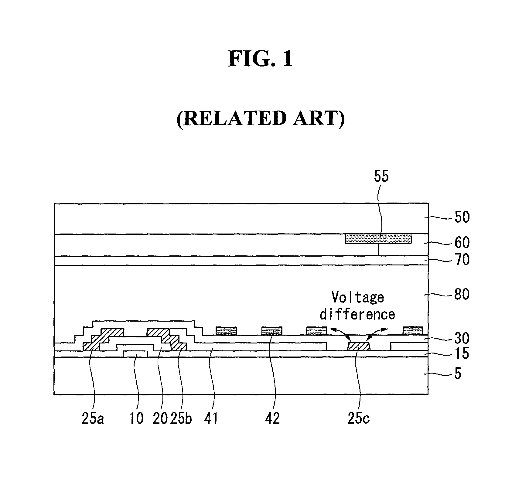
However, when a open circuit failure of the data line was generated, it was difficult to repair the open circuit failure resulting from the shield line positioned on the data line.

Method used


Image

  • Liquid crystal display array substrate and method for manufacturing the same
  • Liquid crystal display array substrate and method for manufacturing the same
  • Liquid crystal display array substrate and method for manufacturing the same

Examples


Embodiment Construction

[0028]Reference will now be made in detail to embodiments of the invention, examples of which are illustrated in the accompanying drawings. Wherever possible, the same reference numbers will be used throughout the drawings to refer to the same or like parts. It will be paid attention that detailed description of known arts will be omitted if it is determined that the arts can mislead the embodiments of the invention.

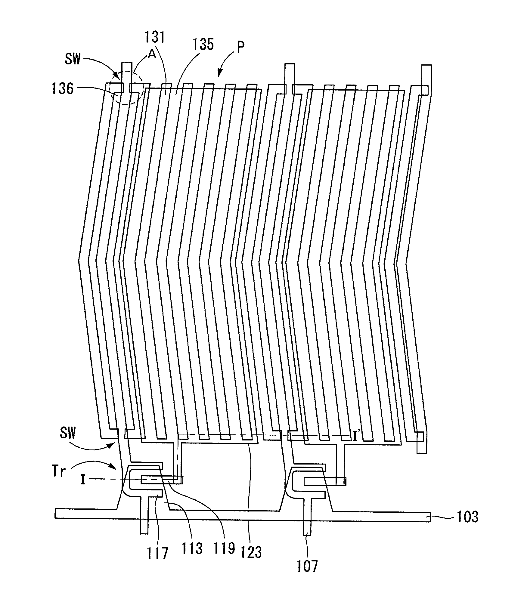
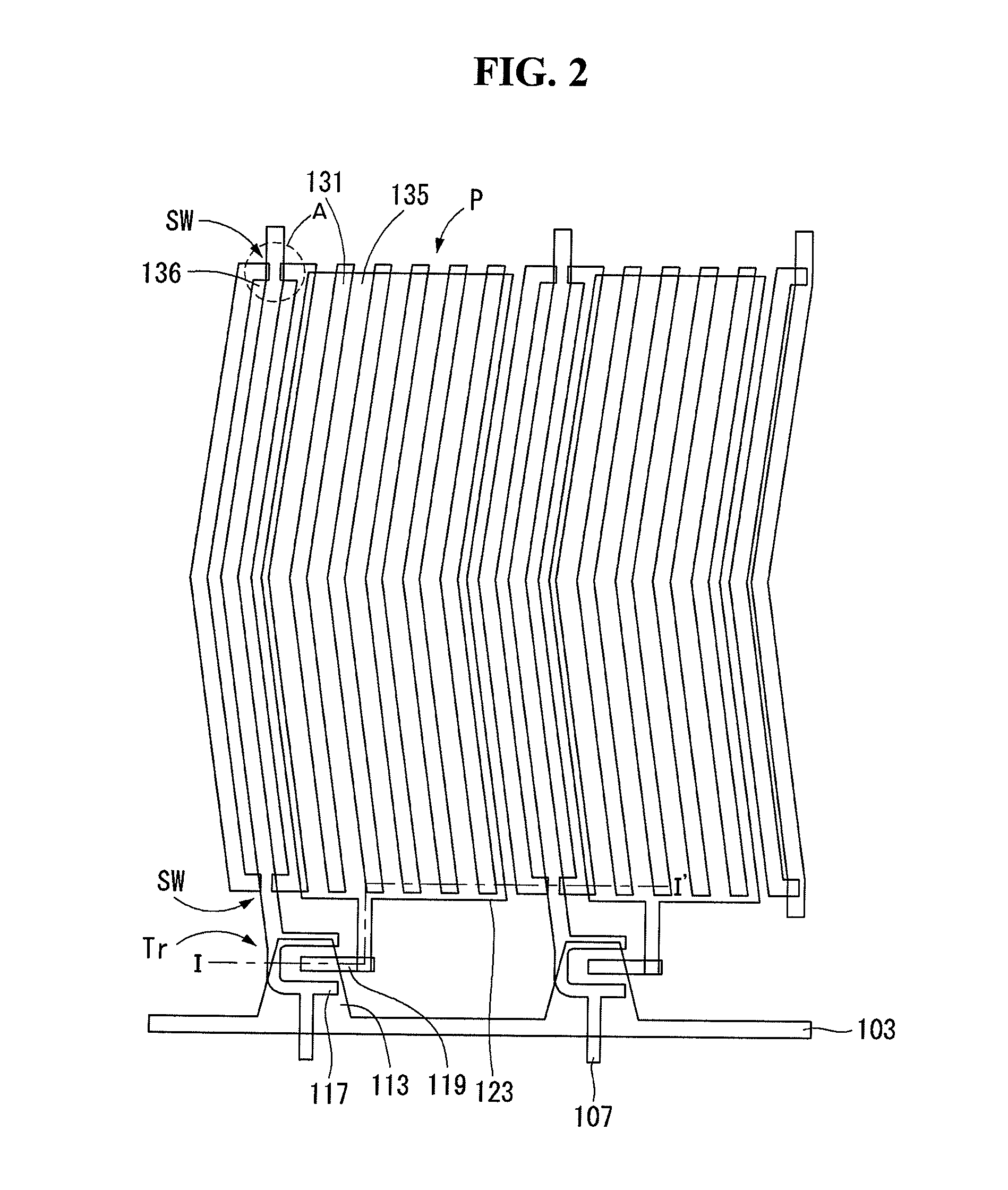
[0029]FIG. 2 is a plane view of an in-plane switching (IPS) mode liquid crystal display (LCD) according to an example embodiment of the invention. FIG. 3 is an enlarged view of an area ‘A’ of FIG. 2. An array substrate and subpixels of the liquid crystal display are shown and described below for the sake of brevity and ease of reading.

[0030]As shown in FIG. 2, a plurality of gate lines 103 are positioned on a substrate (not shown) including a plurality of pixel areas P and extend in one direction. A plurality of data lines 107 is positioned to cross the gate lines 103. H...


PUM

PropertyMeasurementUnit
electric fieldaaaaaaaaaa
widthaaaaaaaaaa
pixel areaaaaaaaaaaa

Abstract

A liquid crystal display array substrate and a method for manufacturing the same are discussed. The liquid crystal display array substrate includes a gate line arranged on a substrate in one direction, a data line which crosses the gate line and defines a plurality of pixel areas, a thin film transistor formed at a crossing of the gate line and the data line, a pixel electrode connected to the thin film transistor, and a common electrode which is positioned opposite the pixel electrode and forms an electric field. The common electrode includes a shield line overlapping the data line, and the shield line includes at least two cutting portions having a width less than other portion of the shield line.

Description

[0001]This application claims the priority benefit of Korean Patent Application No. 10-2012-0023989 filed on Mar. 8, 2012, the entire contents of which is incorporated herein by reference for all purposes as if fully set forth herein.BACKGROUND OF THE INVENTION[0002]1. Field of the Invention[0003]Embodiments of the invention relate to a liquid crystal display, and more specifically, to a liquid crystal display array substrate and a method for manufacturing the same capable of repairing a open circuit failure of data lines.[0004]2. Discussion of the Related Art[0005]Liquid crystal displays are generally driven using optical anisotropy and polarizability of liquid crystals. The liquid crystals have an orientation of molecule arrangement because of their thin and long structure. The liquid crystals may control a direction of molecule arrangement by artificially applying an electric field to the liquid crystals. Thus, if the direction of molecule arrangement of the liquid crystals is ar...

Claims


Application Information

Patent Timeline
Patent Type & Authority Patents(United States)
IPC IPC(8): G02F1/1343G02F1/136H01L29/04
CPCG02F1/134363G02F1/1362G02F2001/136218G02F1/1333H01L27/124H01L21/77G02F1/1368G02F1/136218G02F1/1343
Inventor HWANG, JEONGWOOJEONG, YEONSU
Owner LG DISPLAY CO LTD
Learn More