
Organic light-emitting device with adjustable charge carrier injection

a light-emitting device and charge-carrying technology, which is applied in the direction of static indicating devices, solid-state devices, instruments, etc., can solve the problems of large number of charge-carrying devices, the wrong type of charge-carrying carriers can show a worse lifetime behavior, and the hole or electrons reaching the opposite electrodes are not able to excite the light-emitting molecules, etc., to achieve the effect of more precise adjustment of the width and position

Active Publication Date: 2014-01-14
BEIJING XIAOMI MOBILE SOFTWARE CO LTD
View PDF30 Cites 5 Cited by
  • Summary
  • Abstract
  • Description
  • Claims
  • Application Information

AI Technical Summary

Benefits of technology

[0003]It is therefore an object of the present invention to provide an organic light-emitting device where the injection of charge carriers can be adjusted independently from the operation voltage.
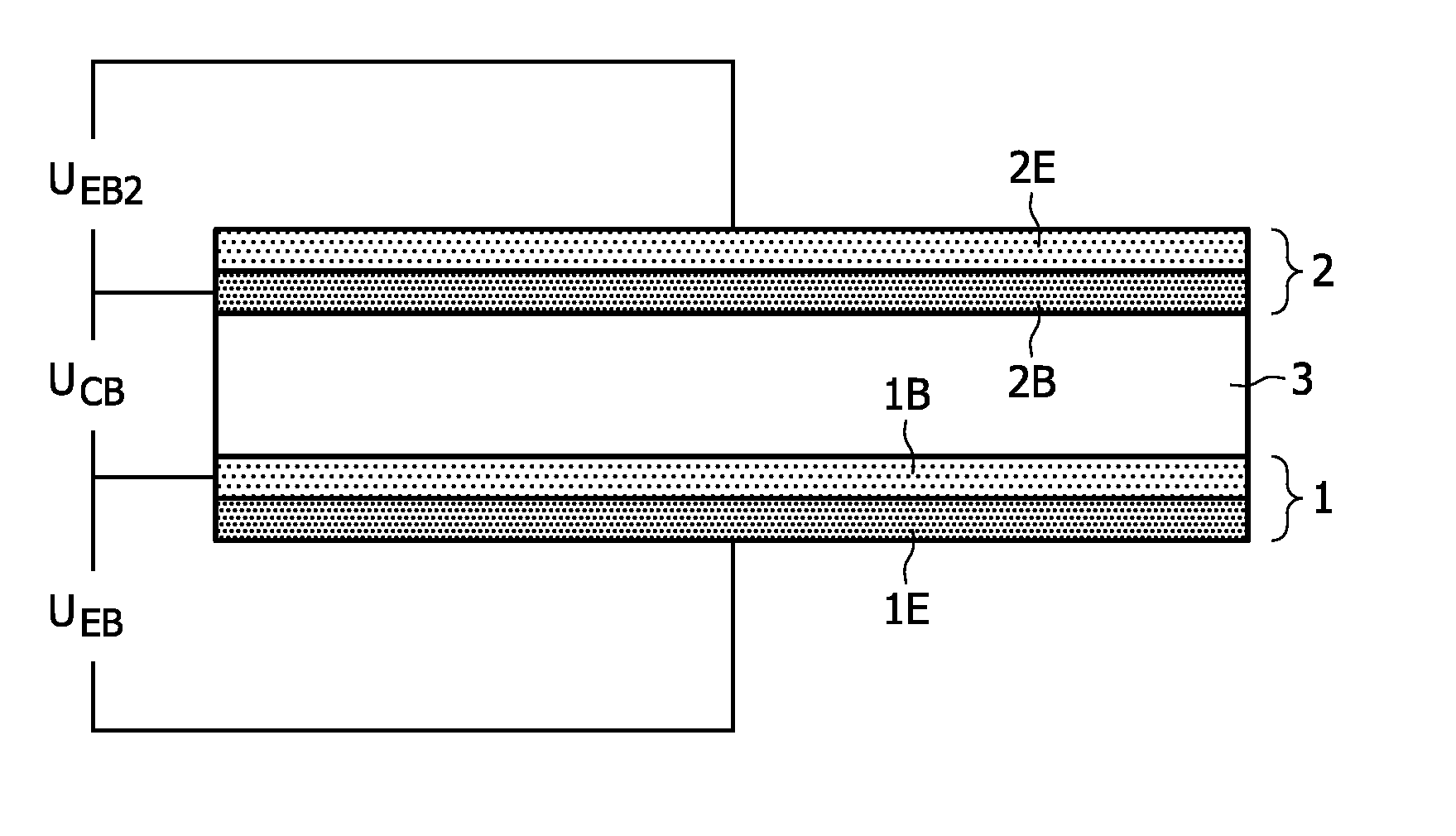
[0013]With independently adjustable charge injection (via UEB) and charge transport (via UCB), position and width of the recombination zone can be varied while maintaining a good charge carrier balance partly predetermined by the present layer stack and layer materials. Variations in layer thickness, material composition, material properties of the organic layer stack leading to the previously described problems can now be easily compensated by suitable adjustment of UEB and UCB. A well-placed recombination zone and a simultaneously well maintained / adjusted charge carrier balance maximize the efficiency w.r.t. light output and minimize negative effects on life-time due to charge carriers penetrating the recombination zone towards the opposite electrode. Eventually, electron and / or hole blocking layers can be avoided because of a well-adjusted charge carrier balance, which reduces the preparation effort and therefore preparation costs. The load of the hole transporting layer with electrons or electron transporting layers with holes can be reduced or ideally avoided. Another advantage is the low required voltage UEB to control the current flow through the organic layer stack. The OLED device according to the present invention is switchable fast between a “light-on” and a “light-off” mode, and the switched base current can be significantly smaller than the total OLED (C and E) current. In the “light-on” mode the second electrode injects charge carriers into the organic layer, while in the “light-off” mode the first electrode injects no charge carriers or a negligible amount of charge carriers into the organic layer. The properties of charge carrier injection of the second electrode will not be influenced by switching the first electrode between light-on mode and light-off mode.
[0017]In another embodiment, the organic light-emitting layer comprises at least a first sub-layer suitable to emit light of a first color and a second sub-layer to emit light of a second color different to the first color. Here, a shift of the recombination zone by suitable adjusting of UEB and UCB enables an adjustment of the color point of the emitted light. For a first set of UEB and UCB, the recombination zone may be located mainly within the first sub-layer leading to a light emission dominated by the first color. For a second set of UEB and UCB, the recombination zone may be located mainly within the second sub-layer leading to a light emission dominated by the second color. The same modification is applicable for three or more different sub-layers emitting light of three or more colors to adjust / modify the color point of the superposed light emitted from the OLED device. To achieve light emission of a certain color, it is also possible to operate the OLED in a switched mode, i.e. modulating the emission color under control of UEB and UCB with a switching frequency high enough to ensure a constant color impression by the human eye.
[0023]First and second voltages UCB and UEB are adjusted independently. Charge carriers are electrons and holes. A suitable separate adjustment of first and second voltage strongly reduces the probability for charge carriers to reach the opposite electrode leading to a more efficient OLED operation. Charge carriers reaching the opposite electrodes are lost for light generation within the organic light-emitting layer. The organic layer stack located between first and second electrode may comprise only one light-emitting layer. In other embodiments, the organic layer stack may comprise additional layers such as hole / electron transport layers, hole / electron injection layers and / or hole / electron blocking layers as well as different organic light-emitting layers emitting light of different colors. Furthermore, the method enables to operate the OLED in a way, where layers mainly designed for transport of one type of charge carriers are at least less loaded with the other type of charge carriers resulting in a better lifetime performance of these layers. The method above may enable to reduce the number of organic layers of an OLED device by avoiding charge carrier blocking layers.
[0024]In an embodiment, the method comprises the step of selecting a suitable first and second voltage to adjusting the position and / or width of a recombination zone to be essentially located within the organic light-emitting layer. In this embodiment, a further improvement of the OLED lifetime will be achieved together with an improved efficiency of the light generation within the organic light-emitting layer. The recombination energy will be released at that location, where the emitting molecules are present. Within the recombination zone, the majority of electrons and holes are bound and therefore cannot penetrate to layers, where the presence of these charge carriers is not desired. The term “essentially” relates to the ratio between thickness of the organic light-emitting layer and the width of the recombination zone. Here, “essentially” corresponds to a ratio of more than 0.8, preferably more than 0.9, more preferred more than 1.0.
[0028]If the injection properties of both charge carriers, electrons and holes, can be controlled via UEB and UEB2, the adjustment of width and position of the recombination zone can be performed more precisely.

Problems solved by technology

Also holes or electrons reaching the opposite electrodes are not able to excite the light-emitting molecules.
Additionally, layers not designed for load with the wrong type of charge carriers could show a worse lifetime behavior.
Additionally, the charge carrier mobility is field or carrier concentration dependent and thus will vary with the applied voltage in a complicated manner.
This could result in a significant number of charge carriers reaching the opposite electrode or stress organic layers only designed for being loaded with the other type of charge carriers.

Method used


Image

  • Organic light-emitting device with adjustable charge carrier injection
  • Organic light-emitting device with adjustable charge carrier injection
  • Organic light-emitting device with adjustable charge carrier injection

Examples


Embodiment Construction

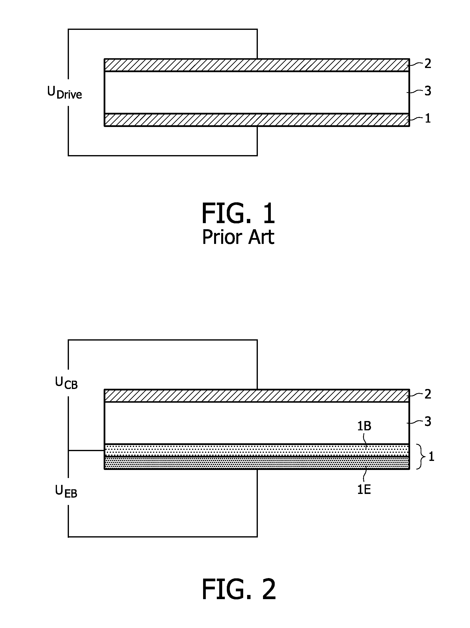
[0037]FIG. 1 shows a side view of an organic light-emitting device according to prior art. The organic light-emitting layer 3 (or layer stack) is arranged between a first electrode 1 and a second electrode 2. In some cases, the organic layer stack comprises only one layer, the organic light-emitting layer 3. In other embodiments, the organic layer stack may comprise additional layers, e.g. hole / electron transport layers, hole / electron injection layers and / or hole / electron blocking layers as well as different organic light-emitting layers emitting light of different colors. The operation voltage UDrive is applied between both electrodes 1 and 2. Assuming electrode 1 as the cathode and electrode 2 as the anode, electrons are injected from cathode 1 while holes are injected from anode 2. The location of the recombination zone (area, where electrons from the cathode and holes from the anode will recombine) depends on structure, design and material properties and applied UDrive. Due to t...


PUM


Abstract

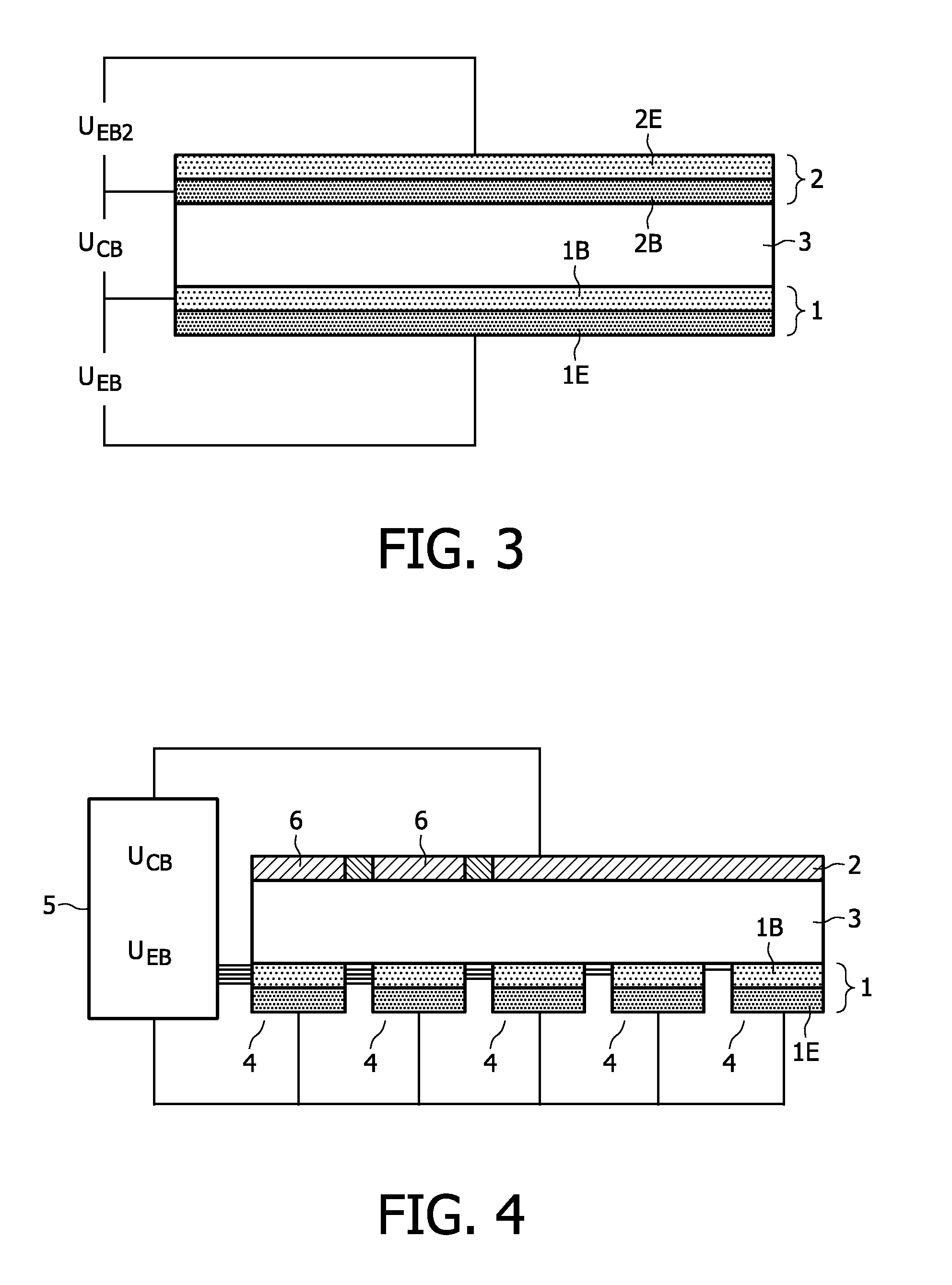
Disclosed is an organic light-emitting device operating similarly to a bipolar transistor. The device includes a collector layer including at least one organic light-emitting layer arranged between a first electrode and a second electrode. The first electrode includes a first emitter layer and a first base layer arranged between the first emitter layer and the collector layer, and the second electrode includes a second emitter layer and a second base layer arranged between the second emitter layer. and the collector layer. In case of a display device, the first emitting layer and the first base layer are structured in order to form an array of pixels of first electrodes suitable to be operated separately by an operation unit in a forward bias mode or a reverse bias mode in order to switch light emission of the EL-layer above each pixel on / off.

Description

FIELD OF THE INVENTION[0001]This invention relates to organic light-emitting devices (OLEDs) and displays comprising such OLEDs with adjustable charge carrier injection and to methods to operate such OLEDs and displays.BACKGROUND OF THE INVENTION[0002]OLEDs are light-emitting devices with a number of layers arranged on top of each other (layer stack) comprising at least one organic light-emitting layer (EL-layer) arranged between two electrodes (anode and cathode). The light is emitted by excited light-emitting molecules (possibly embedded in an organic matrix material) of the EL-layer. The light-emitting molecules are excited by transfer of the recombination energy of electron-hole pairs to the light-emitting molecules within a recombination zone somewhere in the EL-layer. The electrons and holes (charge carriers) are injected from the electrodes into the organic layer stack due to the operating voltage establishing an electric field in the EL layer also responsible for the transpo...

Claims


Application Information

Patent Timeline
Patent Type & Authority Patents(United States)
IPC IPC(8): H01L29/20G09G5/00
CPCH01L51/0504H01L51/5036H01L27/3241H01L51/5203H01L51/5296H10K59/10H10K10/00H10K50/125H10K50/805H10K50/30G09G3/3233G09G3/3291H10K50/814
Inventor LOEBL, HANS-PETERKALISCH, HOLGERJESSEN, FRANK OTTOZIMMERMANN, CHRISTOPH
Owner BEIJING XIAOMI MOBILE SOFTWARE CO LTD
Learn More