
Integrated circuit device, electro optical device and electronic apparatus

a technology of integrated circuits and optical devices, applied in the direction of instruments, computing, electric digital data processing, etc., can solve the problems of display irregularity, display irregularity (streaks) generated luminance irregularity and color irregularity in the displayed image, etc., to prevent display irregularity

Active Publication Date: 2013-12-10
SEIKO EPSON CORP
View PDF10 Cites 1 Cited by
  • Summary
  • Abstract
  • Description
  • Claims
  • Application Information

AI Technical Summary

Benefits of technology

This patent describes a technique to prevent display irregularities in electronic devices, such as screens, televisions, and monitors. The technique involves storing position offset correction values for pixels in the device, and then using those values to correct the position offsets of the data signals. This helps to ensure that the data signals are properly aligned, and reduces display irregularities caused by position offsets or variations in output voltages. Overall, this technique improves the quality and reliability of electronic devices.

Problems solved by technology

As higher definition and higher multiple grayscale are progressed, the higher the multiple grayscale levels, the smaller the grayscale voltage for each grayscale level becomes, which causes a problem in which display irregularity would occur even when a small error occurs in data voltages.
However, the driver of this type entails a problem in which offsets are generated in the multiple data voltages to be multiplex driven.
Due to errors caused by these offsets, there is a problem in that display irregularity (streaks) is generated in the displayed image.
Here, when output voltages of the data line driving circuits have variations, the luminance varies in each of the image regions driven by each of the data line driving circuits, whereby luminance irregularity and color irregularity occurs in displayed images.

Method used


Image

  • Integrated circuit device, electro optical device and electronic apparatus
  • Integrated circuit device, electro optical device and electronic apparatus
  • Integrated circuit device, electro optical device and electronic apparatus

Examples


Embodiment Construction

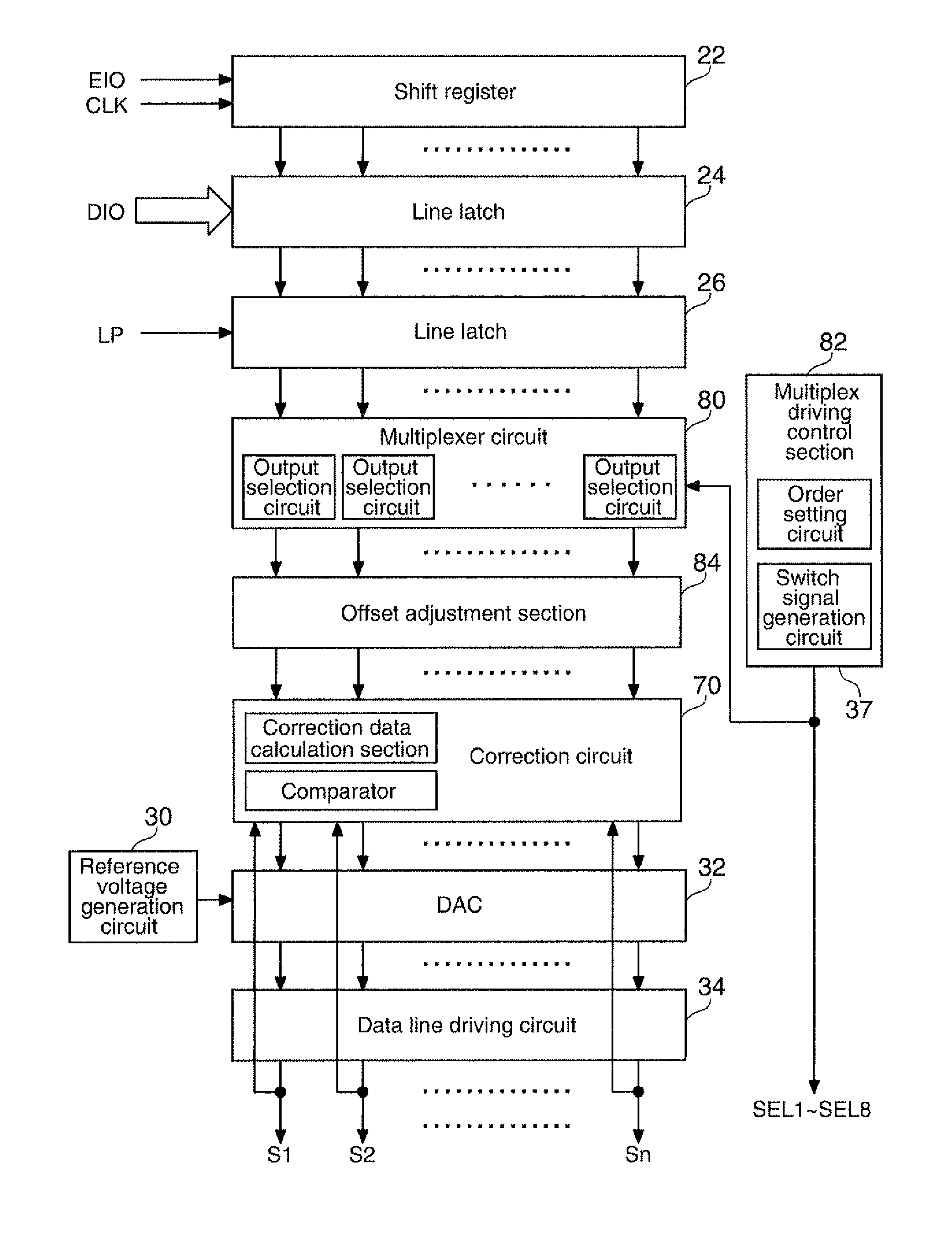
[0066]Preferred embodiments of the invention are described in detail below. It is noted that the embodiments described below do not unduly limit the content of the invention recited in the scope of the claimed invention, and all of the compositions to be described in the embodiments may not necessarily be indispensable as means for solution provided by the invention.

[0067]1. Multiplex Drive

[0068]1.1. Exemplary Composition of Liquid Crystal Display Device

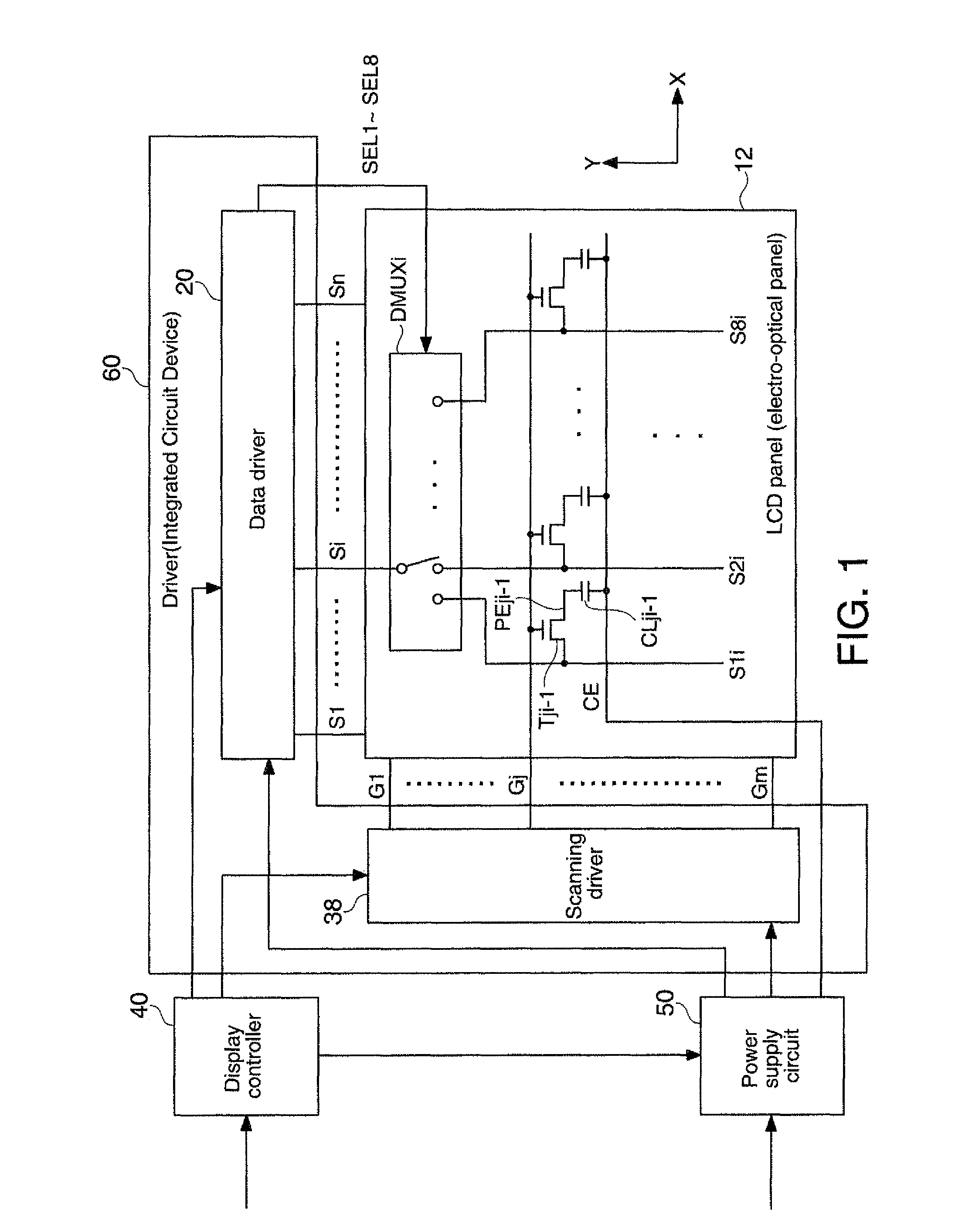
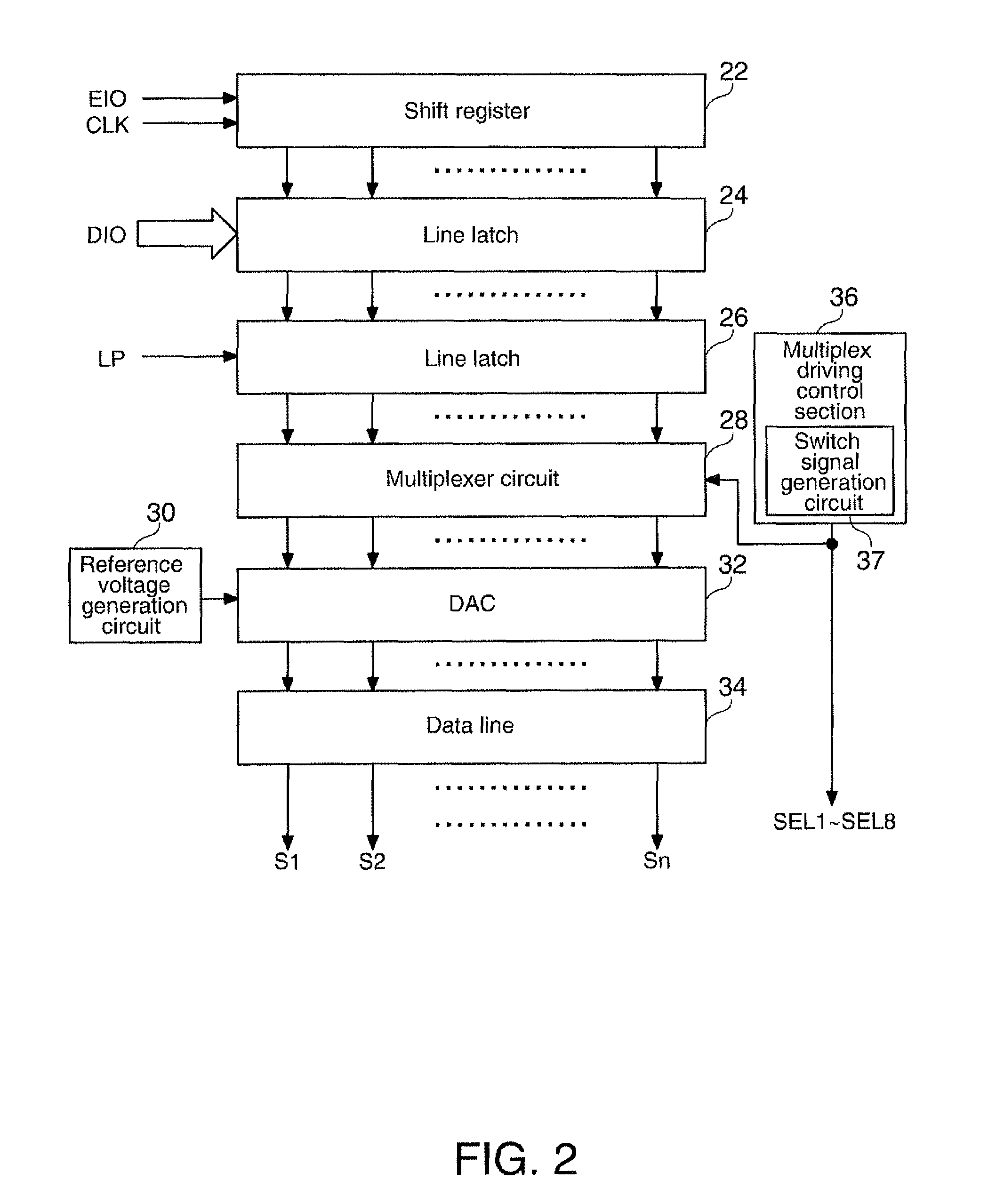
[0069]Referring to FIGS. 1-4, multiplex drive (line sequential drive) performed by the present embodiment will be described.

[0070]Hereinbelow, an example in which a single color display liquid crystal panel that may be used for a liquid crystal projector and the like is driven by a driver (an integrated circuit device) will be described. However, in accordance with an embodiment of the invention, a liquid crystal panel that displays multiple colors such as RGB may be driven by a driver. Also, in accordance with an embodiment of the i...


PUM


Abstract

An integrated circuit device having a data line driving circuit and a position offset addition circuit that connects position offsets based on position offset setting values, wherein, among first pixel to p-th pixel of a plurality of pixels, a position offset register stores a first position offset setting value corresponding to the first pixel and a p-th position offset setting value corresponding to the p-th pixel among the first pixel to the p-th pixel; among first image data to p-th image data respectively corresponding to the first pixel to the p-th pixel, the position offset addition circuit processes a position offset correction value based on the first position offset setting value to the first image data, and processes a position offset correction value based on the p-th position offset setting value to the p-th image data among the first image data to p-th image data, to correct the position offsets.

Description

[0001]The entire disclosure of Japanese Patent Application No. 2009-23170, filed Feb. 4, 2009 is expressly incorporated by reference herein.BACKGROUND[0002]1. Technical Field[0003]An aspect of the present invention relates to integrated circuit devices, electro optical devices and electronic apparatuses.[0004]2. Related Art[0005]In recent years, high definition imaging technology such as high vision imaging have become popular, and higher definition and higher multiple grayscale levels are being pursued for display apparatuses such as liquid crystal projectors and the like. As higher definition and higher multiple grayscale are progressed, the higher the multiple grayscale levels, the smaller the grayscale voltage for each grayscale level becomes, which causes a problem in which display irregularity would occur even when a small error occurs in data voltages.[0006]The applicant has developed a multiplex driving type driver in which each data line driving circuit writes data voltages...

Claims


Application Information

Patent Timeline
Patent Type & Authority Patents(United States)
IPC IPC(8): G06F3/038G09G5/00
CPCG09G3/3688G09G2310/0297G09G2320/0233G09G2320/0285
Inventor MORITA, AKIRA
Owner SEIKO EPSON CORP
Learn More